JAJSQ70D january 2014 – may 2023 TPS65262
PRODUCTION DATA
- 1
- 1 特長
- 2 アプリケーション
- 3 概要
- 4 Revision History
- 5 Pin Configuration and Functions
- 6 Specifications
-
7 Detailed Description
- 7.1 Overview
- 7.2 Functional Block Diagram
- 7.3
Feature Description
- 7.3.1 Adjusting the Output Voltage
- 7.3.2 Enable and Adjusting Undervoltage Lockout
- 7.3.3 Soft-Start Time
- 7.3.4 Power-Up Sequencing
- 7.3.5 V7V Low Dropout Regulator and Bootstrap
- 7.3.6 Out-of-Phase Operation
- 7.3.7 Output Overvoltage Protection (OVP)
- 7.3.8 PSM
- 7.3.9 Slope Compensation
- 7.3.10 Overcurrent Protection
- 7.3.11 Power Good
- 7.3.12 Thermal Shutdown
- 7.4 Device Functional Modes
- 8 Application and Implementation
- 9 Device and Documentation Support
- 10Mechanical, Packaging, and Orderable Information
パッケージ・オプション
メカニカル・データ(パッケージ|ピン)
- RHB|32
サーマルパッド・メカニカル・データ
- RHB|32
発注情報
8.2.2.2 Output Capacitor Selection
There are three primary considerations for selecting the value of the output capacitor. The output capacitor determines the modulator pole, the output voltage ripple, and how the regulator responds to a large change in load current. The output capacitance needs to be selected based on the most stringent of these three criteria.
The desired response to a large change in the load current is the first criteria. The output capacitor needs to supply the load with current when the regulator cannot. This situation can occur if there are desired hold-up times for the regulator where the output capacitor must hold the output voltage above a certain level for a specified amount of time after the input power is removed. The regulator is also temporarily not able to supply sufficient output current if there is a large, fast increase in the current needs of the load such as a transition from no load to full load. The regulator usually needs two or more clock cycles for the control loop to see the change in load current and output voltage and adjust the duty cycle to react to the change. The output capacitor must be sized to supply the extra current to the load until the control loop responds to the load change. The output capacitance must be large enough to supply the difference in current for 2 clock cycles while only allowing a tolerable amount of droop in the output voltage. Equation 10 shows the minimum output capacitance necessary to accomplish this.
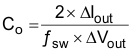
Where ΔIout is the change in output current, ƒsw is the regulator's switching frequency and ΔVout is the allowable change in the output voltage.
Equation 11 calculates the minimum output capacitance needed to meet the output voltage ripple specification.
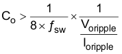
where
- ƒsw is the switching frequency
- Voripple is the maximum allowable output voltage ripple
- Ioripple is the inductor ripple current
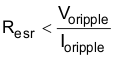
Equation 12 calculates the maximum ESR an output capacitor can have to meet the output voltage ripple specification.
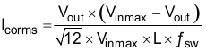
Additional capacitance de-ratings for aging, temperature and DC bias must be factored in which increases this minimum value. Capacitors generally have limits to the amount of ripple current they can handle without failing or producing excess heat. An output capacitor that can support the inductor ripple current must be specified. Some capacitor data sheets specify the root mean square (RMS) value of the maximum ripple current. Equation 13 can be used to calculate the RMS ripple current the output capacitor needs to support.