JAJSNJ1H May   2013  – December 2021 TPS65310A-Q1

PRODUCTION DATA  

  1. 特長
  2. アプリケーション
  3. 概要
  4. Revision History
  5. 概要 (続き)
  6. Pin Configuration and Functions
  7. Specifications
    1. 7.1 Absolute Maximum Ratings
    2. 7.2 ESD Ratings
    3. 7.3 Recommended Operating Conditions
    4. 7.4 Thermal Information
    5. 7.5 Electrical Characteristics
    6. 7.6 SPI Timing Requirements
    7. 7.7 Typical Characteristics
  8. Detailed Description
    1. 8.1 Overview
    2. 8.2 Functional Block Diagram
    3. 8.3 Feature Description
      1. 8.3.1 Buck Controller (Buck1)
        1. 8.3.1.1 Operating Modes
        2. 8.3.1.2 Normal Mode PWM Operation
      2. 8.3.2 Synchronous Buck Converters Buck2 And Buck3
      3. 8.3.3 BOOST Converter
      4. 8.3.4 Frequency-Hopping Spread Spectrum
      5. 8.3.5 Linear Regulator LDO
      6. 8.3.6 Gate Driver Supply
    4. 8.4 Device Functional Modes
      1. 8.4.1  RESET
      2. 8.4.2  Soft Start
      3. 8.4.3  INIT
      4. 8.4.4  TESTSTART
      5. 8.4.5  TESTSTOP
      6. 8.4.6  VTCHECK
      7. 8.4.7  RAMP
      8. 8.4.8  Power-Up Sequencing
      9. 8.4.9  Power-Down Sequencing
      10. 8.4.10 Active
      11. 8.4.11 ERROR
      12. 8.4.12 LOCKED
      13. 8.4.13 LPM0
      14. 8.4.14 Shutdown
        1. 8.4.14.1 Power-On Reset Flag
      15. 8.4.15 Wake Pin
      16. 8.4.16 IRQ Pin
      17. 8.4.17 VBAT Undervoltage Warning
      18. 8.4.18 VIN Over Or Undervoltage Protection
      19. 8.4.19 External Protection
      20. 8.4.20 Overtemperature Detection And Shutdown
      21. 8.4.21 Independent Voltage Monitoring
      22. 8.4.22 GND Loss Detection
      23. 8.4.23 Reference Voltage
      24. 8.4.24 Shutdown Comparator
      25. 8.4.25 LED And High-Side Switch Control
      26. 8.4.26 Window Watchdog
      27. 8.4.27 Timeout In Start-Up Modes
    5. 8.5 Programming
      1. 8.5.1 SPI
        1. 8.5.1.1 FSI Bit
    6. 8.6 Register Maps
      1. 8.6.1 Register Description
      2. 8.6.2 NOP0X00
        1. 8.6.2.1  SPI_SCK_FAIL 0x03
        2. 8.6.2.2  LPMO_CMD 0x11
        3. 8.6.2.3  LOCK_CMD 0x12
        4. 8.6.2.4  PWR_STAT 0x21
        5. 8.6.2.5  SYS_STAT 0x22
        6. 8.6.2.6  SPI_STAT 0x23
        7. 8.6.2.7  COMP_STAT 0x24
        8. 8.6.2.8  DEV_REV 0x2F
        9. 8.6.2.9  PWR_CONFIG 0x31
        10. 8.6.2.10 DEV_CONFIG 0x32
        11. 8.6.2.11 CLOCK_CONFIG 0x33
  9. Application and Implementation
    1. 9.1 Application Information
    2. 9.2 Typical Applications
      1. 9.2.1 Buck Controller 1
        1. 9.2.1.1 Design Requirements
        2. 9.2.1.2 Detailed Design Procedure
          1. 9.2.1.2.1 Adjusting the Output Voltage for the BUCK1 Controller
          2. 9.2.1.2.2 Output Inductor, Sense Resistor and Capacitor Selection for the BUCK1 Controller
          3. 9.2.1.2.3 Compensation of the Buck Controller
          4. 9.2.1.2.4 Bootstrap Capacitor for the BUCK1 Controller
        3. 9.2.1.3 BUCK 1 Application Curve
      2. 9.2.2 Synchronous Buck Converters BUCK2 and BUCK3
        1. 9.2.2.1 Design Requirements
        2. 9.2.2.2 Detailed Design Procedure
          1. 9.2.2.2.1 Adjusting the Output Voltage for the BUCK2 and BUCK3 Converter
          2. 9.2.2.2.2 Output Inductor Selection for the BUCK2 and BUCK3 Converter
          3. 9.2.2.2.3 Compensation of the BUCK2 and BUCK3 Converters
          4. 9.2.2.2.4 Bootstrap Capacitor for the BUCK2/3 Converters
        3. 9.2.2.3 Application Curves
      3. 9.2.3 BOOST Converter
        1. 9.2.3.1 Design Requirements
        2. 9.2.3.2 Detailed Design Procedure
          1. 9.2.3.2.1 Adjusting the Output Voltage for the Boost Converter
          2. 9.2.3.2.2 Output Inductor and Capacitor Selection for the BOOST Converter
          3. 9.2.3.2.3 Compensation of the BOOST Converter
          4. 9.2.3.2.4 Output Diode for the BOOST Converter
        3. 9.2.3.3 BOOST Converter Application Curves
      4. 9.2.4 Linear Regulator
        1. 9.2.4.1 Design Requirements
        2. 9.2.4.2 Detailed Design Procedure
          1. 9.2.4.2.1 Adjusting the Output Voltage for the Linear Regulator
          2. 9.2.4.2.2 Output Capacitance for the Linear Regulator
        3. 9.2.4.3 Linear Regulator Application Curve
  10. 10Power Supply Recommendations
  11. 11Layout
    1. 11.1 Layout Guidelines
      1. 11.1.1 Buck Controller
      2. 11.1.2 Buck Converter
      3. 11.1.3 Boost Converter
      4. 11.1.4 Linear Regulator
      5. 11.1.5 Other Considerations
    2. 11.2 Layout Example
  12. 12Device and Documentation Support
    1. 12.1 Documentation Support
      1. 12.1.1 Related Documentation
    2. 12.2 Receiving Notification of Documentation Updates
    3. 12.3 サポート・リソース
    4. 12.4 Trademarks
    5. 12.5 Electrostatic Discharge Caution
    6. 12.6 Glossary
  13. 13Mechanical, Packaging, and Orderable Information

パッケージ・オプション

メカニカル・データ(パッケージ|ピン)
サーマルパッド・メカニカル・データ
発注情報
Output Inductor, Sense Resistor and Capacitor Selection for the BUCK1 Controller

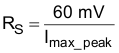
An external resistor senses the current through the inductor. The current sense resistor pins (S1 and S2) are fed into an internal differential amplifier which supports the range of VBUCK1 voltages. The sense resistor RS must be chosen so that the maximum forward peak current in the inductor generates a voltage of 75 mV across the sense pins. This specified typical value is for low duty cycles only. At typical duty-cycle conditions around 28% (assuming 3.8-V output and 12-V input), 60 mV is a more reasonable value, considering tolerances and mismatches. The typical characteristics (see Figure 7-2) provide a guide for using the correct current-limit sense voltage.

Equation 14. GUID-C9D10DC6-F9BB-45BE-A14B-E9EF605C260A-low.gif

Optimal slope compensation which is adaptive to changes in input voltage and duty cycle allows stable operation at all conditions. In order to specify optimal performance of this circuit, the following condition must be satisfied in the choice of inductor and sense resistor:

Equation 3. GUID-DD176B78-55B3-4D2B-88ED-0B2BDE17DAD7-low.gif

where

  • L = inductor in µH
  • Rs = sense resistor in Ω

The current sense pins S1 and S2 are high impedance pins with low leakage across the entire VBUCK1 range. This allows DCR current sensing (see Figure 8-2) using the DC resistance of the inductor for better efficiency.

For selecting the output capacitance and its ESR resistance, the following set of equations can be used:
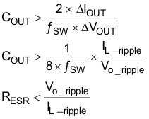
Equation 4. GUID-CDAD9E61-335E-47CC-B209-ACD57D8707F2-low.gif

where

  • ƒsw is the 490-kHz switching frequency
  • ΔIOUT is the worst-case load step from the application
  • ΔVOUT is the allowed voltage step on the output
  • Vo_ripple is the allowed output voltage ripple
  • IL_ripple is the ripple current in the coil