JAJS410N December 2005 – November 2016 TPS74201
PRODUCTION DATA.
- 1 特長
- 2 アプリケーション
- 3 概要
- 4 改訂履歴
- 5 Pin Configuration and Functions
- 6 Specifications
- 7 Detailed Description
- 8 Application and Implementation
- 9 Power Supply Recommendations
- 10Layout
- 11デバイスおよびドキュメントのサポート
- 12メカニカル、パッケージ、および注文情報
パッケージ・オプション
メカニカル・データ(パッケージ|ピン)
サーマルパッド・メカニカル・データ
発注情報
8 Application and Implementation
NOTE
Information in the following applications sections is not part of the TI component specification, and TI does not warrant its accuracy or completeness. TI’s customers are responsible for determining suitability of components for their purposes. Customers should validate and test their design implementation to confirm system functionality.
8.1 Application Information
8.1.1 Input, Output, and Bias Capacitor Requirements
The TPS742 family does not require any output capacitor for stability. If an output capacitor is needed, the device is designed to be stable for all available types and values of output capacitance. The device is also stable with multiple capacitors in parallel, which can be of any type or value.
The capacitance required on the IN and BIAS pins is strongly dependent on the input supply source impedance. To counteract any inductance in the input, the minimum recommended capacitor for VIN and VBIAS is 1μF. If VIN and VBIAS are connected to the same supply, the recommended minimum capacitor for VBIAS is 4.7 μF. Use good quality, low ESR capacitors on the input; ceramic X5R and X7R capacitors are preferred. Place these capacitors as close to the pins as possible for optimum performance.
8.1.2 Transient Response
The TPS742 family of devices were designed to have transient response within 5% for most applications without any output capacitor. In some cases, the transient response may be limited by the transient response of the input supply. This limitation is especially true in applications where the difference between the input and output is less than 300 mV. In this case, adding additional input capacitance improves the transient response much more than just adding additional output capacitance would do. With a solid input supply, adding additional output capacitance reduces undershoot and overshoot during a transient at the expense of a slightly longer VOUT recovery time. See Figure 20 in the Typical Characteristics section. Because the TPS742 devices are stable without an output capacitor, many applications may allow for little or no capacitance at the LDO output. For these applications, local bypass capacitance for the device under power may be sufficient to meet the transient requirements of the application. This design reduces the total solution cost by avoiding the need to use expensive high-value capacitors at the LDO output.
8.1.3 Dropout Voltage
The TPS742 family of devices offers industry-leading dropout performance, making this family well-suited for high-current low VIN/low VOUT applications. The extremely low dropout of the TPS742 allows the device to be used in place of a DC-DC converter and still achieve good efficiency. This efficiency allows the user to rethink the power architecture for their applications to achieve the smallest, simplest, and lowest cost solution.
There are two different specifications for dropout voltage with the TPS742 devices. The first specification (illustrated in Figure 24) is referred to as VIN Dropout, and is for users who wish to apply an external bias voltage to achieve low dropout. This specification assumes that VBIAS is at least 1.62 V above VOUT, which is the case for VBIAS when powered by a 3.3-V rail with 5% tolerance and with VOUT = 1.5 V. If VBIAS is higher than 3.3 V × 0.95 or VOUT is less than 1.5 V, VIN dropout is less than specified.
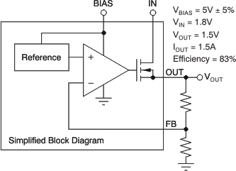 Figure 24. Typical Application of the TPS742 Using an Auxiliary Bias Rail
The second specification (shown in Figure 25) is referred to as VBIAS Dropout, and is for users who wish to tie IN and BIAS together. This option allows the device to be used in applications where an auxiliary bias voltage is not available or low dropout is not required. Dropout is limited by BIAS in these applications because VBIAS provides the gate drive to the pass FET and therefore must be 1.4 V above VOUT. Because of this usage, IN and BIAS tied together easily consume huge power. Pay attention not to exceed the power rating of the IC package.
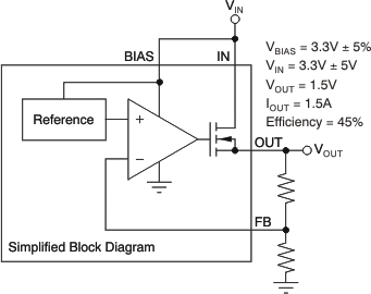 Figure 25. Typical Application of the TPS742 Without an Auxiliary Bias
8.1.4 Output Noise
The TPS742 devices provide low-output noise when a soft-start capacitor is used. When the device reaches the end of the soft-start cycle, the soft-start capacitor serves as a filter for the internal reference. By using a 0.001-μF soft-start capacitor, the output noise is reduced by half and is typically 30 μVRMS for a 1.2-V output (10 Hz to 100 kHz). Because most of the output noise is generated by the internal reference, the noise is a function of the set output voltage. The RMS noise with a 0.001-μF soft-start capacitor is given in Equation 1.

The low-output noise of the TPS742 makes the device a good choice for powering transceivers, PLLs, or other noise-sensitive circuitry.
8.1.5 Programmable Soft-Start
The TPS742 devices feature a programmable, monotonic, voltage-controlled soft start that is set with an external capacitor (CSS). This feature is important for many applications, because power-up initialization problems are eliminated when powering FPGAs, DSPs, or other processors. The controlled voltage ramp of the output also reduces peak inrush current during start-up, minimizing start-up transients to the input power bus.
To achieve a linear and monotonic soft-start, the TPS742 error amplifier tracks the voltage ramp of the external soft-start capacitor until the voltage exceeds the internal reference. The soft-start ramp time depends on the soft-start charging current (ISS), soft-start capacitance (CSS), and the internal reference voltage (VREF), and can be calculated using Equation 2:

If large output capacitors are used, the device current limit (ICL) and the output capacitor may set the start-up time. In this case, the start-up time is given by Equation 3:

VOUT(NOM) is the nominal set output voltage as set by the user, COUT is the output capacitance, and ICL(MIN) is the minimum current limit for the device. In applications where monotonic start-up is required, the soft-start time given by Equation 2 must be set to be greater than Equation 3.
The maximum recommended soft-start capacitor is 0.015 μF. Larger soft-start capacitors can be used and do not damage the device; however, the soft-start capacitor discharge circuit may not be able to fully discharge the soft-start capacitor when enabled. Soft-start capacitors larger than 0.015 μF could be a problem in applications where the user must rapidly pulse the enable pin and still requires the device to soft-start from ground. CSS must be low-leakage; X7R, X5R, or C0G dielectric materials are preferred. See Table 2 for suggested soft-start capacitor values.
Table 2. Standard Capacitor Values for Programming the Soft-Start Time
(See Equation 4)
| CSS | SOFT-START TIME |
|---|---|
| Open | 0.1 ms |
| 470 pF | 0.5 ms |
| 1000 pF | 1 ms |
| 4700 pF | 5 ms |
| 0.01 μF | 10 ms |
| 0.015 μF | 16 ms |
8.1.6 Sequencing Requirements
The device can have VIN, VBIAS, and VEN sequenced in any order without causing damage to the device. However, for the soft-start function to work as intended, certain sequencing rules must be applied. Enabling the device after VIN and VBIAS are present is preferred, and can be accomplished using a digital output from a processor or supply supervisor. An analog signal from an external RC circuit, as shown in Figure 26, can also be used as long as the delay time is long enough for VIN and VBIAS to be present.
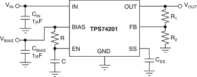 Figure 26. Soft-Start Delay Using an RC Circuit on Enable
If a signal is not available to enable the device after IN and BIAS, simply connecting EN to IN is acceptable for most applications as long as VIN is greater than 1.1 V and the ramp rate of VIN and VBIAS is faster the set soft-start ramp rate. If the ramp rate of the input sources is slower than the set soft-start time, the output tracks the slower supply minus the dropout voltage until the set output voltage is reached. If EN is connected to BIAS, the device does soft-start as programmed provided that VIN is present before VBIAS. If VBIAS and VEN are present before VIN is applied and the set soft-start time has expired then VOUT tracks VIN.
NOTE
When VBIAS and VEN are present and VIN is not supplied, this device outputs approximately 50 μA of current from OUT. Although this condition will not cause any damage to the device, the output current may charge up the OUT node if total resistance between OUT and GND (including external feedback resistors) is greater than 10 kΩ..
8.2 Typical Applications
Figure 27 is a typical application circuit for the TPS742 adjustable output device.
R1 and R2 can be calculated for any output voltage using the formula shown in Figure 27. See Table 3 for sample resistor values of common output voltages. To achieve the maximum accuracy specifications, R2 must be ≤ 4.99 kΩ.
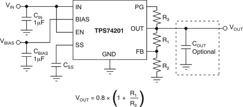 Figure 27. Typical Application Circuit for the TPS742
Table 3. Standard 1% Resistor Values for Programming the Output Voltage
(See Equation 5)
| R1 (kΩ) | R2 (kΩ) | VOUT (V) |
|---|---|---|
| Short | Open | 0.8 |
| 0.619 | 4.99 | 0.9 |
| 1.13 | 4.53 | 1 |
| 1.37 | 4.42 | 1.05 |
| 1.87 | 4.99 | 1.1 |
| 2.49 | 4.99 | 1.2 |
| 4.12 | 4.75 | 1.5 |
| 3.57 | 2.87 | 1.8 |
| 3.57 | 1.69 | 2.5 |
| 3.57 | 1.15 | 3.3 |
NOTE
When VBIAS and VEN are present and VIN is not supplied, this device outputs approximately 50 μA of current from OUT. Although this condition does not cause any damage to the device, the output current can charge up the OUT node if total resistance between OUT and GND (including external feedback resistors) is greater than 10 kΩ.
8.2.1 Design Requirements
The design goals are VIN = 1.8 V, VOUT = 1.5 V, and IOUT = 1 A (maximum). The design optimizes transient response and meets a 1-ms start-up time with a start-up dominated by the soft-start feature. The input supply comes from a supply on the same circuit board. The available system rails for VBIAS are 2.7 V, 3.3 V, and 5 V.
The design space consists of CIN, COUT, CBIAS, CSS, VBIAS, R1, R2, and R3, and the circuit is from Figure 27.
This example uses a VIN of 1.8 V, with a VBIAS of 2.5 V.
8.2.2 Detailed Design Procedure
This is assuming the table for the standard capacitor values is put back in as Table 1.
Utilizing Table 3, we select R1 = 4.12 kΩ for VOUT = 1.5 V. and R2 = 4.75 kΩ. Using Table 1, we select CSS = 1000 pF for a 1-ms typical start-up time. For optimal performance, we use the 5-V rail for a Bias supply. An R3 of 100 kΩ is selected as the PG bus is used by other devices with additional 100-kΩ pullup resistors.
A CIN of 10 µF is used for better transient performance on the input supply, a CBIAS of 1 µF is used to ensure the Bias supply is solid, and a COUT of 1 µF is used to provide some local capacitance on the output.
8.2.3 Application Curves
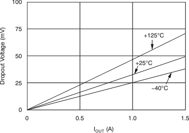 Figure 28. VIN Dropout Voltage vs
 IOUT and Temperature (TJ)
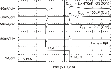 Figure 30. Output Load Transient Response
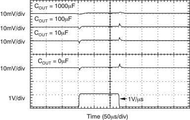
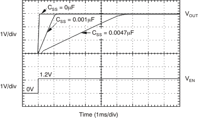 Figure 31. Turnon Response
