JAJSQ10E march 2012 – may 2023 TPS7A16-Q1
PRODUCTION DATA
- 1
- 1 特長
- 2 アプリケーション
- 3 説明
- 4 Revision History
- 5 Pin Configuration and Functions
- 6 Specifications
- 7 Detailed Description
-
8 Application and Implementation
- 8.1 Application Information
- 8.2 Typical Applications
- 8.3 Power Supply Recommendations
- 8.4 Layout
- 9 Device and Documentation Support
- 10Mechanical, Packaging, and Orderable Information
パッケージ・オプション
メカニカル・データ(パッケージ|ピン)
- DGN|8
サーマルパッド・メカニカル・データ
- DGN|8
発注情報
8.2.3 Multicell Battery Packs
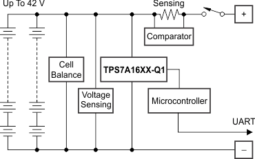
Currently, battery packs can employ up to a dozen cells in series that, when fully charged, can have voltages of up to 55 V. Internal circuitry in these battery packs is used to prevent overcurrent and overvoltage conditions that can degrade battery life or even pose a safety risk; this internal circuitry is often managed by a low-power microcontroller, such as TI’s MSP430™. See the overview for microcontrollers (MCU) for more information.
The microcontroller continuously monitors the battery, whether the battery is in use or not. Although this microcontroller can be powered by an intermediate voltage taken from the multicell array, this approach unbalances the battery pack, degrading the battery life or adding cost to implement more complex cell-balancing topologies.
The best approach to power this microcontroller is to regulate down the voltage from the entire array to discharge every cell equally and prevent any balancing issues. This approach reduces system complexity and cost.
The TPS7A16-Q1 can be used for this application because this device can handle very high voltages (from the entire multicell array) and has very low quiescent current (to maximize battery life).
 Figure 8-6 Protection Based on Low-Power Microcontroller Power From Multicell Battery Packs