JAJSE12A October   2017  – October 2017 TPS92830-Q1

PRODUCTION DATA.  

  1. 特長
  2. アプリケーション
  3. 概要
    1.     概略回路図
  4. 改訂履歴
  5. 概要(続き)
  6. Pin Configuration and Functions
    1.     Pin Functions
  7. Specifications
    1. 7.1 Absolute Maximum Ratings
    2. 7.2 ESD Ratings
    3. 7.3 Recommended Operating Conditions
    4. 7.4 Thermal Information
    5. 7.5 Electrical Characteristics
    6. 7.6 Timing Requirements
    7. 7.7 Typical Characteristics
  8. Detailed Description
    1. 8.1 Overview
    2. 8.2 Functional Block Diagram
    3. 8.3 Feature Description
      1. 8.3.1 Device Bias
        1. 8.3.1.1 Power-On-Reset (POR)
        2. 8.3.1.2 Current Reference (IREF)
        3. 8.3.1.3 Low-Current Fault Mode
      2. 8.3.2 Charge Pump
        1. 8.3.2.1 Charge Pump Architecture
      3. 8.3.3 Constant-Current Driving
        1. 8.3.3.1 High-Side Current Sense
        2. 8.3.3.2 High-Side Current Driving
        3. 8.3.3.3 Gate Overdrive Voltage Protection
        4. 8.3.3.4 High-Precision Current Regulation
        5. 8.3.3.5 Parallel MOSFET Driving
      4. 8.3.4 PWM Dimming
        1. 8.3.4.1 Supply Dimming
        2. 8.3.4.2 PWM Dimming by Input
        3. 8.3.4.3 Internal Precision PWM Generator
        4. 8.3.4.4 Full Duty-Cycle Switch
      5. 8.3.5 Analog Dimming
        1. 8.3.5.1 Analog Dimming Topology
        2. 8.3.5.2 Internal High-Precision Pullup Current Source
      6. 8.3.6 Output Current Derating
        1. 8.3.6.1 Output-Current Derating Topology
      7. 8.3.7 Diagnostics and Fault
        1. 8.3.7.1 LED Short-to-GND Detection
        2. 8.3.7.2 LED Short-to-GND Auto Retry
        3. 8.3.7.3 LED Open-Circuit Detection
        4. 8.3.7.4 LED Open-Circuit Auto Retry
        5. 8.3.7.5 Dropout-Mode Diagnostics
        6. 8.3.7.6 Overtemperature Protection
        7. 8.3.7.7 FAULT Bus Output With One-Fails–All-Fail
        8. 8.3.7.8 Fault Table
    4. 8.4 Device Functional Modes
      1. 8.4.1 Undervoltage Lockout, V(IN) < V(UVLO)
      2. 8.4.2 Normal Operation (V(IN) ≥ 4.5 V, V(IN) > V(LED) + 0.5 V)
      3. 8.4.3 Low-Voltage Dropout
      4. 8.4.4 Fault Mode (Fault Is Detected)
  9. Application and Implementation
    1. 9.1 Application Information
    2. 9.2 Typical Applications
      1. 9.2.1 Typical Application for Automotive Exterior Lighting With One-Fails–All-Fail
        1. 9.2.1.1 Design Requirements
        2. 9.2.1.2 Detailed Design Procedure
        3. 9.2.1.3 Application Curves
      2. 9.2.2 High-Precision Dual-Brightness PWM Generation
        1. 9.2.2.1 Dual-Brightness Application
        2. 9.2.2.2 Design Requirements
        3. 9.2.2.3 Detailed Design Procedure
        4. 9.2.2.4 Application Curve
      3. 9.2.3 Driving High-Current LEDs With Parallel MOSFETs
        1. 9.2.3.1 Application Curves
  10. 10Layout
    1. 10.1 Layout Guidelines
    2. 10.2 Layout Example
  11. 11デバイスおよびドキュメントのサポート
    1. 11.1 ドキュメントの更新通知を受け取る方法
    2. 11.2 コミュニティ・リソース
    3. 11.3 商標
    4. 11.4 静電気放電に関する注意事項
    5. 11.5 Glossary
  12. 12メカニカル、パッケージ、および注文情報

パッケージ・オプション

メカニカル・データ(パッケージ|ピン)
サーマルパッド・メカニカル・データ
発注情報

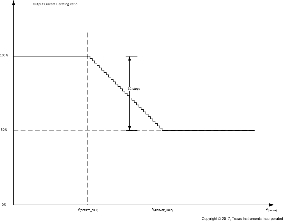
Output-Current Derating Topology

Voltage at the DERATE pin, V(DERATE), is used for output-current-derating control. To set the V(DERATE) voltage, a resistor divider on supply voltage VIN is typically used for supply overvoltage protection.

  • When VDERATE is lower than V(DERATE_FULL), output current derating is not enabled; thus, output-current derating ratio k(DERATE_Dim) is at 100%.
  • When VDERATE is higher than V(DERATE_HALF), output current derating is limited to 50%; thus, output-current derating ratio k(DERATE_Dim) is at 50%.
  • When V(DERATE) is between V(DERATE_FULL) and V(DERATE_HALF), the output-current-derating ratio is negatively proportional to V(DERATE) with 32 steps. Current derating is rounded to the next-lower step. The output-current-derating ratio can be calculated using the following equations.
  • Equation 8. TPS92830-Q1 Equation_06_SLIS178.gif
    Equation 9. TPS92830-Q1 Equation_07_SLIS178.gif
TPS92830-Q1 Output_Current_Derating_Profile_SLIS178.gifFigure 28. Output-Current Derating Profile