JAJSFO6F December 2015 – April 2019 TPS99000-Q1
PRODUCTION DATA.
- 1 特長
- 2 アプリケーション
- 3 概要
- 4 改訂履歴
- 5 概要(続き)
- 6 Pin Configuration and Functions
-
7 Specifications
- 7.1 Absolute Maximum Ratings
- 7.2 ESD Ratings
- 7.3 Recommended Operating Conditions
- 7.4 Thermal Information
- 7.5 Electrical Characteristics - Transimpedance Amplifier Parameters
- 7.6 Electrical Characteristics - Digital to Analog Converters
- 7.7 Electrical Characteristics - Analog to Digital Converter
- 7.8 Electrical Characteristics - FET Gate Drivers
- 7.9 Electrical Characteristics - Photo Comparator
- 7.10 Electrical Characteristics - Voltage Regulators
- 7.11 Electrical Characteristics - Temperature and Voltage Monitors
- 7.12 Electrical Characteristics - Current Consumption
- 7.13 Power-Up Timing Requirements
- 7.14 Power-Down Timing Requirements
- 7.15 Timing Requirements - Sequencer Clock
- 7.16 Timing Requirements - Host / Diagnostic Port SPI Interface
- 7.17 Timing Requirements - ADC Interface
- 7.18 Switching Characteristics
-
8 Detailed Description
- 8.1 Overview
- 8.2 Functional Block Diagram
- 8.3
Feature Description
- 8.3.1
Illumination Control
- 8.3.1.1 Illumination System High Dynamic Range Dimming Overview
- 8.3.1.2 Illumination Control Loop
- 8.3.1.3 Continuous Mode Operation
- 8.3.1.4
Discontinuous Mode Operation
- 8.3.1.4.1 Discontinuous Mode Pulse Width Limit
- 8.3.1.4.2 COMPOUT_LOW Timer in Discontinuous Operation
- 8.3.1.4.3 Dimming Within Discontinuous Operation Range
- 8.3.1.4.4 Multiple Pulse Heights to Increase Bit Depth
- 8.3.1.4.5 TIA Gain Adjustment
- 8.3.1.4.6 Current Limit in Discontinuous Mode
- 8.3.1.4.7 CMODE Big Cap Mode in Discontinuous Operation
- 8.3.2 Over-Brightness Detection
- 8.3.3 Analog to Digital Converter
- 8.3.4 Power Sequencing and Monitoring
- 8.3.5 DMD Mirror Voltage Regulator
- 8.3.6 Low Dropout Regulators
- 8.3.7 System Monitoring Features
- 8.3.8 Communication Ports
- 8.3.1
Illumination Control
- 8.4 Device Functional Modes
- 8.5 Register Maps
- 9 Application and Implementation
- 10Power Supply Recommendations
- 11Layout
- 12デバイスおよびドキュメントのサポート
- 13メカニカル、パッケージ、および注文情報
パッケージ・オプション
メカニカル・データ(パッケージ|ピン)
- PZP|100
サーマルパッド・メカニカル・データ
- PZP|100
発注情報
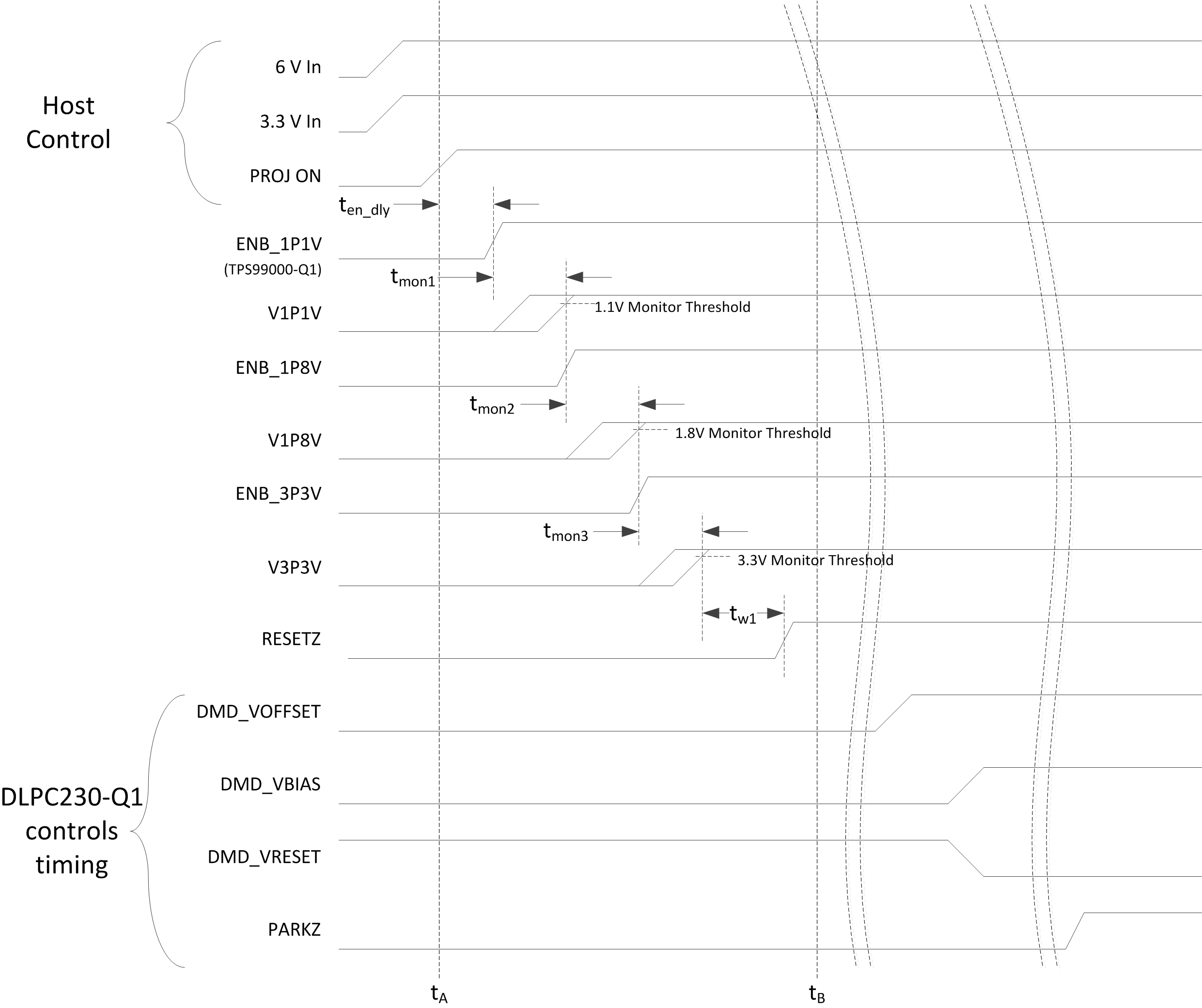
7.13 Power-Up Timing Requirements
| TYP | UNIT | |||
|---|---|---|---|---|
| ten_dly | PROJ_ON to 1.1 V enable. This includes PROJ_ON tglitch time. | Rising edge of PROJ_ON to rising edge of 1.1 V enable. | 11 | ms |
| tmon1(1)(2) | Maximum time for 1.1 V rail to reach voltage threshold after enable has been asserted. This delay length will occur even if 1.1 V meets threshold earlier. | Rising edge of ENB_1P1V to internal 1.1 V monitor test. | 10 | ms |
| tmon2(1)(2) | Maximum time for 1.8 V rail to reach voltage threshold after enable has been asserted. This delay length will occur even if 1.8 V meets threshold earlier. | Rising edge of ENB_1P8V to internal 1.8 V monitor test. | 10 | ms |
| tmon3(1)(2) | Maximum time for 3.3 V rail to reach voltage threshold after enable has been asserted. This delay length will occur even if 3.3 V meets threshold earlier. | Rising edge of ENB_3P3V to internal 3.3 V monitor test. | 10 | ms |
| tw1 | RESETZ delay after voltage testing completion. | Completion of 3.3 V monitor test to RESETZ rising edge. | 10 | ms |
(1) V1P1V, V1P8V, and V3P3V rails can be enabled prior to the TPS99000-Q1 assertion of their respective enable signal if required for system power design. If necessary, ENB_1P1V may be connected to the 1.1 V, 1.8 V, and 3.3 V external supply enables.
(2) If any voltage threshold is not met within the specified time, the TPS99000-Q1 will not de-assert RESETZ. The power-up procedure must be fully restarted in this situation.
 Figure 1. Power Up Timing