JAJSG15C June   2015  – August 2018 TUSB321

PRODUCTION DATA.  

  1. 特長
  2. アプリケーション
  3. 概要
    1.     Device Images
      1.      概略回路図
      2.      サンプル・アプリケーション
  4. 改訂履歴
  5. Pin Configuration and Functions
    1.     Pin Functions
  6. Specifications
    1. 6.1 Absolute Maximum Ratings
    2. 6.2 ESD Ratings
    3. 6.3 Recommended Operating Conditions
    4. 6.4 Thermal Information
    5. 6.5 Electrical Characteristics
    6. 6.6 Switching Characteristics
  7. Detailed Description
    1. 7.1 Overview
      1. 7.1.1 Cables, Adapters, and Direct Connect Devices
        1. 7.1.1.1 USB Type-C Receptacles and Plugs
        2. 7.1.1.2 USB Type-C Cables
        3. 7.1.1.3 Legacy Cables and Adapters
        4. 7.1.1.4 Direct Connect Devices
    2. 7.2 Functional Block Diagram
    3. 7.3 Feature Description
      1. 7.3.1 Port Role Configuration
        1. 7.3.1.1 Downstream Facing Port (DFP) - Source
        2. 7.3.1.2 Upstream Facing Port (UFP) - Sink
        3. 7.3.1.3 Dual Role Port (DRP)
      2. 7.3.2 Type-C Current Mode
      3. 7.3.3 VBUS Detection
      4. 7.3.4 Cable Orientation and External MUX Control
      5. 7.3.5 VCONN Support for Active Cables
    4. 7.4 Device Functional Modes
      1. 7.4.1 Unattached Mode
      2. 7.4.2 Active Mode
  8. Application and Implementation
    1. 8.1 Application Information
    2. 8.2 Typical Application
      1. 8.2.1 DFP Mode
        1. 8.2.1.1 Design Requirements
        2. 8.2.1.2 Detailed Design Procedure
        3. 8.2.1.3 Application Curve
    3. 8.3 Initialization Set Up
  9. Power Supply Recommendations
  10. 10Layout
    1. 10.1 Layout Guidelines
    2. 10.2 Layout Example
  11. 11デバイスおよびドキュメントのサポート
    1. 11.1 ドキュメントの更新通知を受け取る方法
    2. 11.2 コミュニティ・リソース
    3. 11.3 商標
    4. 11.4 静電気放電に関する注意事項
    5. 11.5 Glossary
  12. 12メカニカル、パッケージ、および注文情報

パッケージ・オプション

メカニカル・データ(パッケージ|ピン)
サーマルパッド・メカニカル・データ
発注情報

Switching Characteristics

over operating free-air temperature range (unless otherwise noted)
PARAMETER MIN TYP MAX UNIT
tCCCB_DEFAULT Power on default of CC1 and CC2 voltage debounce time 133 ms
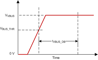
tVBUS_DB Debounce of VBUS_DET pin after valid VBUS_THR (See Figure 1.) 2 ms
tDRP_DUTY_CYCLE Power-on default of percentage of time DRP advertises DFP during a TDRP 30%
tDRP The period TUSB321 in DFP mode completes a DFP to UFP and back advertisement. 50 75 100 ms
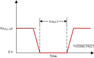
tFAULT VCONN_FAULT asserted low time after VCONN over-current condition is detected. (See Figure 2.) 7 10 13 µs
TUSB321 tvbus_db_sllseo6.gifFigure 1. VBUS Detect and Debounce
TUSB321 vconn_fault_sllseo6.gifFigure 2. VCONN_FAULT Assertion Pulse Timing