JAJSCK9B september 2016 – december 2021 UCC21521
PRODUCTION DATA
- 1
- 1 特長
- 2 アプリケーション
- 3 概要
- 4 Revision History
- 5 Pin Configuration and Functions
-
6 Specifications
- 6.1 Absolute Maximum Ratings
- 6.2 ESD Ratings
- 6.3 Recommended Operating Conditions
- 6.4 Thermal Information
- 6.5 Power Ratings
- 6.6 Insulation Specifications
- 6.7 Safety-Related Certifications
- 6.8 Safety-Limiting Values
- 6.9 Electrical Characteristics
- 6.10 Switching Characteristics
- 6.11 Insulation Characteristics Curves
- 6.12 Typical Characteristics
- 7 Parameter Measurement Information
- 8 Detailed Description
-
9 Application and Implementation
- 9.1 Application Information
- 9.2
Typical Application
- 9.2.1 Design Requirements
- 9.2.2
Detailed Design Procedure
- 9.2.2.1 Designing INA/INB Input Filter
- 9.2.2.2 Select External Bootstrap Diode and its Series Resistor
- 9.2.2.3 Gate Driver Output Resistor
- 9.2.2.4 Gate to Source Resistor Selection
- 9.2.2.5 Estimate Gate Driver Power Loss
- 9.2.2.6 Estimating Junction Temperature
- 9.2.2.7 Selecting VCCI, VDDA/B Capacitor
- 9.2.2.8 Dead Time Setting Guidelines
- 9.2.2.9 Application Circuits with Output Stage Negative Bias
- 9.2.3 Application Curves
- 10Power Supply Recommendations
- 11Layout
- 12Device and Documentation Support
- 13Mechanical, Packaging, and Orderable Information
パッケージ・オプション
メカニカル・データ(パッケージ|ピン)
- DW|16
サーマルパッド・メカニカル・データ
- DW|16
発注情報
9.2.2.6 Estimating Junction Temperature
The junction temperature (TJ) of the UCC21521 can be estimated with:
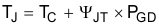
where
- TC is the UCC21521 case-top temperature measured with a thermocouple or some other instrument, and
- ΨJT is the Junction-to-case-top thermal resistance from the Thermal Information table.
Using the junction-to-top characterization parameter (ΨJT) instead of the junction-to-case thermal resistance (RΘJC) can greatly improve the accuracy of the junction temperature estimation. The majority of the thermal energy of most ICs is released into the PCB through the package leads, whereas only a small percentage of the total energy is released through the top of the case (where thermocouple measurements are usually conducted). RΘJC can only be used effectively when most of the thermal energy is released through the case, such as with metal packages or when a heatsink is applied to an IC package. In all other cases, use of RΘJC will inaccurately estimate the true junction temperature. ΨJT is experimentally derived by assuming that the amount of energy leaving through the top of the IC will be similar in both the testing environment and the application environment. As long as the recommended layout guidelines are observed, junction temperature estimates can be made accurately to within a few degrees Celsius. For more information, see the Semiconductor and IC Package Thermal Metrics application report.