JAJSHT2C august 2019 – december 2020 UCC28740-Q1
PRODUCTION DATA
- 1
- 1 特長
- 2 アプリケーション
- 3 概要
- 4 Revision History
- 5 Revision History
- 6 Revision History
- 7 Pin Configuration and Functions
- 8 Specifications
- 9 Detailed Description
-
10Application and Implementation
- 10.1 Application Information
- 10.2 High Voltage Applications
- 10.3
Typical Application
- 10.3.1 Design Requirements
- 10.3.2
Detailed Design Procedure
- 10.3.2.1 Custom Design With WEBENCH® Tools
- 10.3.2.2 Standby Power Estimate and No-Load Switching Frequency
- 10.3.2.3 Input Bulk Capacitance and Minimum Bulk Voltage
- 10.3.2.4 38
- 10.3.2.5 Transformer Turns-Ratio, Inductance, Primary Peak Current
- 10.3.2.6 Transformer Parameter Verification
- 10.3.2.7 VS Resistor Divider, Line Compensation
- 10.3.2.8 Output Capacitance
- 10.3.2.9 VDD Capacitance, CVDD
- 10.3.2.10 Feedback Network Biasing
- 10.3.3 Application Curves
- 11Power Supply Recommendations
- 12Layout
-
13Device and Documentation Support
- 13.1
Device Support
- 13.1.1 Development Support
- 13.1.2
Device Nomenclature
- 13.1.2.1 Capacitance Terms in Farads
- 13.1.2.2 Duty Cycle Terms
- 13.1.2.3 Frequency Terms in Hertz
- 13.1.2.4 Current Terms in Amperes
- 13.1.2.5 Current and Voltage Scaling Terms
- 13.1.2.6 Transformer Terms
- 13.1.2.7 Power Terms in Watts
- 13.1.2.8 Resistance Terms in Ohms
- 13.1.2.9 Timing Terms in Seconds
- 13.1.2.10 Voltage Terms in Volts
- 13.1.2.11 AC Voltage Terms in VRMS
- 13.1.2.12 Efficiency Terms
- 13.2 Documentation Support
- 13.3 Receiving Notification of Documentation Updates
- 13.4 Community Resources
- 13.5 Trademarks
- 13.1
Device Support
- Mechanical, Packaging, and Orderable Information
10.3.3 Application Curves
The transient response shown in Figure 10-3 was taken with a 115 VAC, 60 Hz input voltage and a load transition from 0 A to full load. Channel 1 is the load current on a scale of 1 A per division, channel 4 is the otutput voltage on a scale of 1 V per division. The cursor shows the minimum acceptable voltage limit, 4.30 V, under transient conditions. Also note that the output waveform was taken with the probe on TP5 with the ground referenced to TP4 but not using the tip and barrel technique accounting for the high frequency noise seen on the waveform.
The typical switching waveform can be seen in Figure 10-4. Channel 1 shows the VS pin at 2 V per division and channel 2 shows the MOSFET drain to source voltage at 100 V per division. The scan was taken at 1.8-A load, 115-VAC, 60-Hz input voltage. At this operating point, the switching frequency is dithering between 58.8 kHz and 52.6 kHz due to valley skipping.
The UCC28740-Q1 controller employs a unique control mechanism to help with EMI compliance. As shown in Figure 10-5, the DRV pin, shown as channel 3, drives the gate of the MOSFET with a sequence of pulses in which there will be two longer pulses, two medium pulses, and two shorter pulses at any operating point starting with the amplitude modulation mode. The EMI dithering is not enabled at light load. Figure x shows the result of these varying pulse widths on the CS signal, shown on channel 4. The longer pulses result in a peak current threshold of 808 mV, the medium length pulses are shown measured at 780 mV, and the shorter pulses measure a threshold voltage of 752 mV. This dithering adds to the frequency jitter caused by valley skipping and results in a spread spectrum for better EMI compliance.
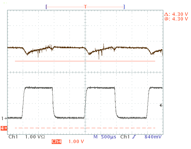
| 115 VAC, 60 Hz | 0 A to 2 A | |
| CH 1 = Load Current, 1 A/DIV | ||
| CH 4 = VOUT, cursor shows minimum limit | ||
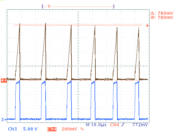 Figure 10-5 EMI Dithering
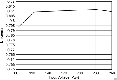 Figure 10-7 Average Efficiency
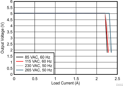 Figure 10-9 VOUT vs. IOUT
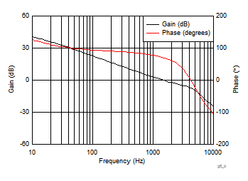
| VIN = 115 VAC | IOUT = 2 A |
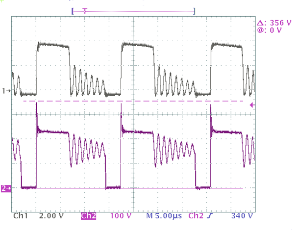
| CH 1 = VS | CH 2 = VDS | |
| IOUT = 1.8 A | VIN = 115 VAC, 60 Hz | |
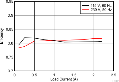
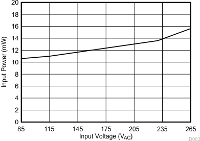 Figure 10-8 No Load Power Consumption
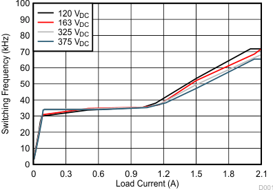 Figure 10-10 Control Law