JAJSSI7J August 2001 – December 2023 UCC29002 , UCC39002
PRODUCTION DATA
- 1
- 1特長
- 2アプリケーション
- 3概要
- 4Pin Configuration and Functions
- 5Specifications
-
6Detailed Description
- 6.1 Overview
- 6.2 Functional Block Diagram
- 6.3
Feature Description
- 6.3.1 Differential Current-Sense Amplifier (CS+, CS−, CSO)
- 6.3.2 Load-Share Bus Driver Amplifier (CSO, LS)
- 6.3.3 Load-Share Bus Receiver Amplifier (LS)
- 6.3.4 Error Amplifier (EAO)
- 6.3.5 Adjust Amplifier Output (ADJ)
- 6.3.6 Enable Function (CS+, CS−)
- 6.3.7 Fault Protection on LS Bus
- 6.3.8 Start-Up and Adjust Logic
- 6.3.9 Bias Input and Bias_OK Circuit (VDD)
- 6.4 Device Functional Modes
- 7Application and Implementation
- 8Device and Documentation Support
- 9Revision History
- Mechanical, Packaging, and Orderable Information
パッケージ・オプション
メカニカル・データ(パッケージ|ピン)
サーマルパッド・メカニカル・データ
発注情報
7.3.1 Measuring the Voltage Loop of a Power Module
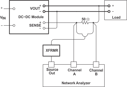
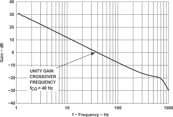
Using the test configuration shown in Figure 7-4, measure the unity-gain crossover frequency of each power module to be paralleled. Set the load to the maximum output current (IOUT(max)) to be shared by each module. Figure 7-5 shows a typical resultant Bode plot. Select the plot with the lowest 0dB crossover frequency and assign that frequency to fCO(module) for design use.
 Figure 7-4 Connection Diagram for Unity-Gain Crossover Frequency Measurement
  Figure 7-5 Power
Module Bode Plot