SLUSDC1 September 2018 UCD90320U
PRODUCTION DATA.
- 1 Features
- 2 Applications
- 3 Description
- 4 Revision History
- 5 Description Continued
- 6 Pin Configuration and Functions
- 7 Specifications
-
8 Detailed Description
- 8.1 Overview
- 8.2 Functional Block Diagram
- 8.3 Feature Description
- 8.4
Device Functional Modes
- 8.4.1 Rail Monitoring Configuration
- 8.4.2 GPI Configuration
- 8.4.3 Rail Sequence Configuration
- 8.4.4 Fault Responses Configuration
- 8.4.5 GPO Configuration
- 8.4.6 Margining Configuration
- 8.4.7 Pin Selected Rail States Configuration
- 8.4.8 Watchdog Timer
- 8.4.9 System Reset Function
- 8.4.10 Cascading Multiple Devices
- 8.4.11 Rail Monitoring
- 8.4.12 Status Monitoring
- 8.4.13 Data and Error Logging to EEPROM Memory
- 8.4.14 Black Box First Fault Logging
- 8.4.15 PMBus Address Selection
- 8.4.16 ADC Reference
- 8.4.17 Device Reset
- 8.4.18 Brownout
- 8.4.19 Internal Fault Management
- 8.4.20 Single Event Upset
- 8.5 Device Configuration and Programming
- 9 Application and Implementation
- 10Power Supply Recommendations
- 11Layout
- 12Device and Documentation Support
- 13Mechanical, Packaging, and Orderable Information
11.2 Layout Example
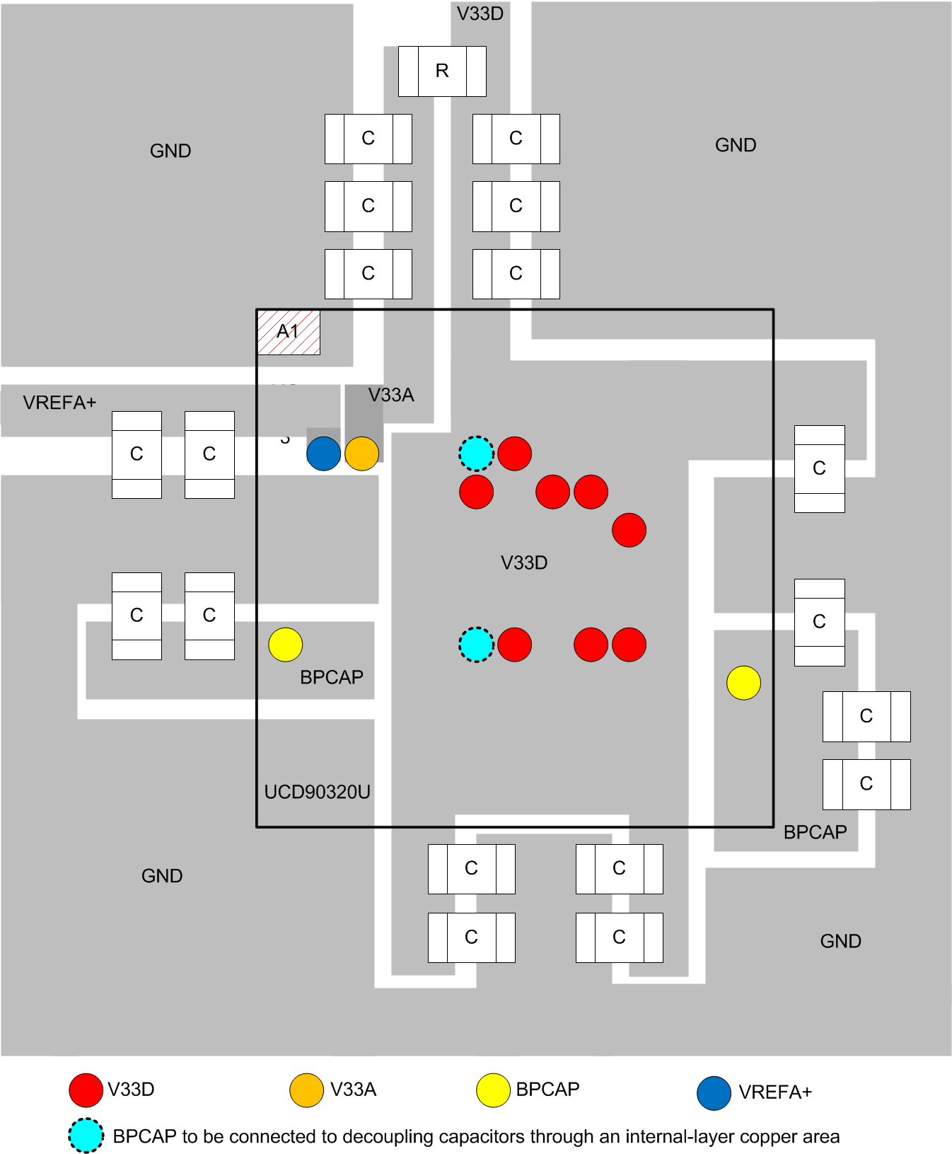
The UCD90320U device is available in a 169-pin BGA package. If the design calls for the device to be mounted on the top layer, decoupling capacitors can be placed on the bottom layer to allow room for top-layer trace routing. The layout example below describes this strategy. Figure 43 shows bottom-layer component placement from top-view. In addition to Figure 43, consider these important suggestions.
- Use a uniform ground plane to connect DVSS, AVSS, and VREFA– pins.
- Connect all four BPCAP pins to a common internal-layer copper area.
- AVSS and VREFA– pins can be connected to a common internal-layer copper area.
Figure 43 shows a typical application with the UCD90320U device mounted on the top layer and the components placed on the bottom layer.
 Figure 43. Layout Example