JAJSES0 February 2018 XTR305
PRODUCTION DATA.
- 1 特長
- 2 アプリケーション
- 3 概要
- 4 改訂履歴
- 5 Pin Configuration and Functions
-
6 Specifications
- 6.1 Absolute Maximum Ratings
- 6.2 ESD Ratings
- 6.3 Recommended Operating Conditions
- 6.4 Thermal Information
- 6.5 Electrical Characteristics: Voltage Output Mode
- 6.6 Electrical Characteristics: Current Output Mode
- 6.7 Electrical Characteristics: Operational Amplifier (OPA)
- 6.8 Electrical Characteristics: Instrumentation Amplifier (IA)
- 6.9 Electrical Characteristics: Current Monitor
- 6.10 Electrical Characteristics: Power and Digital
- 6.11 Typical Characteristics
- 7 Detailed Description
-
8 Application and Implementation
- 8.1 Application Information
- 8.2
Typical Application
- 8.2.1 Design Requirements
- 8.2.2
Detailed Design Procedure
- 8.2.2.1 Voltage Output Mode
- 8.2.2.2 Current Output Mode
- 8.2.2.3 Input Signal Connection
- 8.2.2.4 Externally-Configured Mode: OPA and IA
- 8.2.2.5 Driver Output Disable
- 8.2.2.6 Driving Capacitive Loads and Loop Compensation
- 8.2.2.7 Internal Current Sources, Switching Noise, and Settling Time
- 8.2.2.8 IA Structure, Voltage Monitor
- 8.2.2.9 Digital I/O and Ground Considerations
- 8.2.2.10 Output Protection
- 8.2.3 Application Curves
- 9 Power Supply Recommendations
- 10Layout
- 11デバイスおよびドキュメントのサポート
- 12メカニカル、パッケージ、および注文情報
8.2.2.8 IA Structure, Voltage Monitor
The instrumentation amplifier has high-impedance NPN transistor inputs that do not load the output signal, which is especially important in current output mode. The output signal is a controlled current that is multiplexed either to the SET pin (to close the voltage output loop) or to IAOUT (for external access).
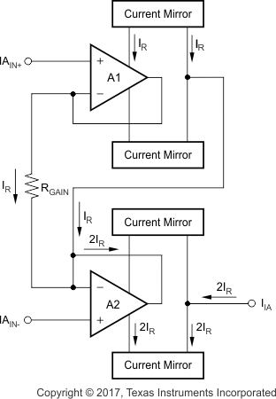
The principal circuit is shown in Figure 44. The two input buffer amplifiers reproduce the input difference voltage across RGAIN. The resulting current through this resistor is bidirectionally mirrored to the output. That mirroring results in the transfer function of Equation 6:

The accuracy and drift of RGAIN defines the accuracy of the voltage to current conversion. The high accuracy and stability of the current mirrors result from a cycling chopper technique.
 Figure 44. IA Block Diagram
 The output current, IAOUT, of the instrumentation amplifier is limited to protect the internal circuitry. This current limit has two settings controlled by the state of M2 (see Electrical Characteristics: Instrumentation Amplifier (IA), Short-Circuit Current specification).
NOTE
If RSET is too small, the current output limitation of the instrumentation amplifier can disrupt the closed loop of the XTR305 in voltage output mode.
With M2 = low, the nominal RGAIN of 10 kΩ allows an input voltage of 20 VPP, which produces an output current of 4 mAPP. When using lower resistors for RGAIN that can allow higher currents, the IA output current limitation must be taken into account.