JAJSC12D October   2013  – April 2018 TPS7B67-Q1

PRODUCTION DATA.  

  1. 特長
  2. アプリケーション
  3. 概要
    1.     Device Images
      1.      可変出力オプション
      2.      固定出力オプション
  4. 改訂履歴
  5. 概要(続き)
  6. Device Comparison
  7. Pin Configuration and Functions
    1.     Pin Functions
  8. Specifications
    1. 8.1 Absolute Maximum Ratings
    2. 8.2 ESD Ratings
    3. 8.3 Recommended Operating Conditions
    4. 8.4 Thermal Information
    5. 8.5 Electrical Characteristics
    6. 8.6 Timing Requirements
    7. 8.7 Typical Characteristics
  9. Detailed Description
    1. 9.1 Overview
    2. 9.2 Functional Block Diagrams
    3. 9.3 Feature Description
      1. 9.3.1 Enable (EN)
      2. 9.3.2 Regulated Output (VOUT)
      3. 9.3.3 Power-On-Reset (RESET)
      4. 9.3.4 Reset Delay Timer (DELAY)
      5. 9.3.5 Adjustable Output Voltage (ADJ for TPS7B6701)
      6. 9.3.6 Undervoltage Shutdown
      7. 9.3.7 Thermal Shutdown
      8. 9.3.8 Thermal Protection
    4. 9.4 Device Functional Modes
      1. 9.4.1 Operation With VIN < 4 V
      2. 9.4.2 Operation With EN Control
  10. 10Application and Implementation
    1. 10.1 Application Information
    2. 10.2 Typical Application
      1. 10.2.1 Design Requirements
      2. 10.2.2 Detailed Design Procedure
        1. 10.2.2.1 Power Dissipation and Thermal Considerations
      3. 10.2.3 Application Curves
  11. 11Power Supply Recommendations
    1. 11.1 Dropout Recovery
      1. 11.1.1 LDO Dropout Recovery Explained
      2. 11.1.2 TPS7B67xx-Q1 Dropout During Startup
  12. 12Layout
    1. 12.1 Layout Guidelines
      1. 12.1.1 Enhanced Thermal Pad
      2. 12.1.2 Package Mounting
      3. 12.1.3 Board Layout Recommendations to Improve PSRR and Noise Performance
      4. 12.1.4 Additional Layout Considerations
    2. 12.2 Layout Example
  13. 13デバイスおよびドキュメントのサポート
    1. 13.1 関連リンク
    2. 13.2 ドキュメントの更新通知を受け取る方法
    3. 13.3 コミュニティ・リソース
    4. 13.4 商標
    5. 13.5 静電気放電に関する注意事項
    6. 13.6 Glossary
  14. 14メカニカル、パッケージ、および注文情報

TPS7B67xx-Q1 Dropout During Startup

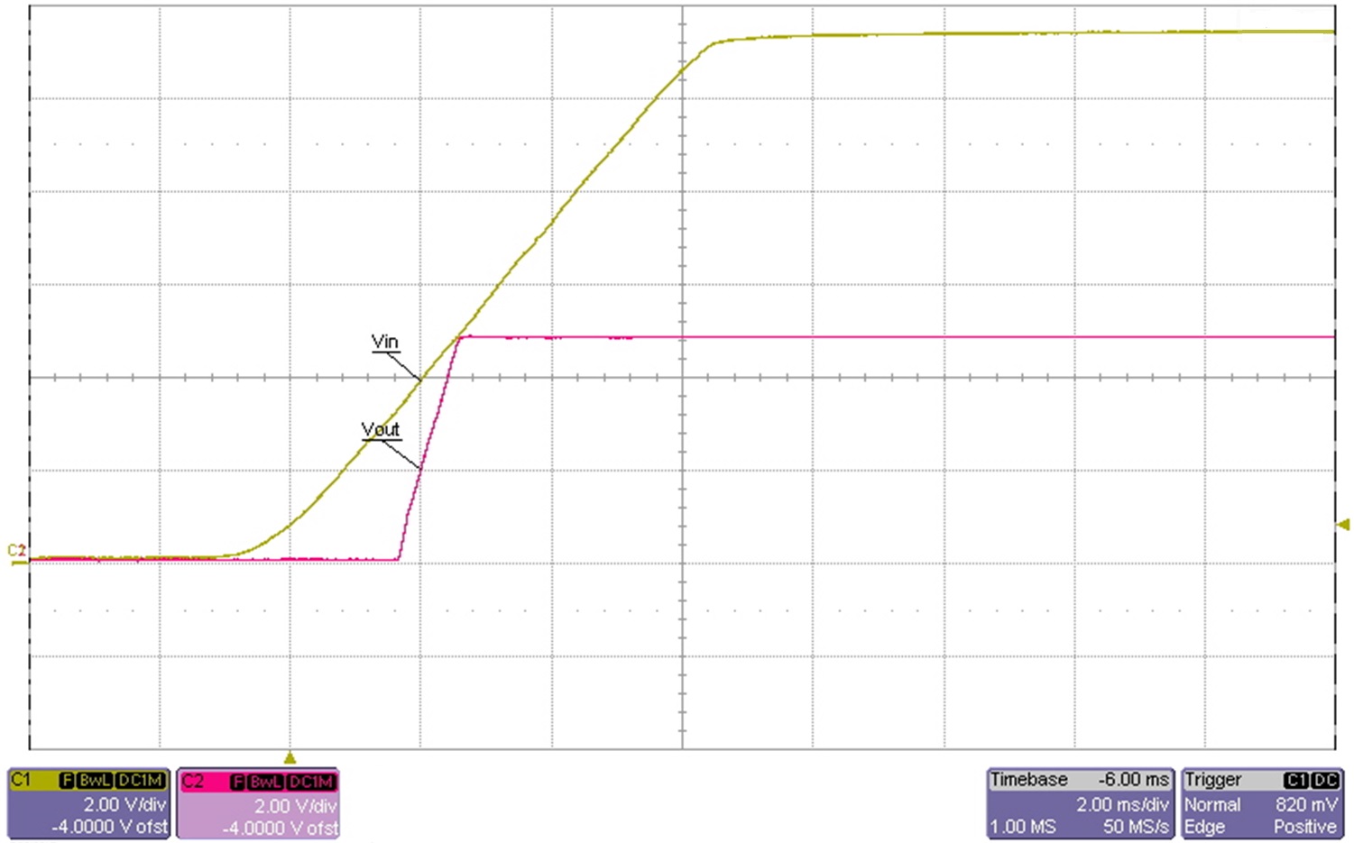
The TPS7B67xx-Q1 does not overshoot significantly if the LDO is enabled after the input voltage is already above VOUT(NOM) plus VDO. Furthermore, startup performance is not affected as long as the input voltage transitions from VUVLO+(IN) to VOUT(NOM) plus VDO in less than 1 millisecond. Approximately 1 millisecond is required for the TPS7B67xx-Q1 reference voltage to reach its steady state value, so input voltage startup transitions that are less than 1 millisecond do not force the device into dropout. One example that does not overshoot is a 5-V output voltage with full load (full load has the highest dropout), where the input voltage ramps steadily from 0 V to 5.45 V in less than 3 milliseconds. Overshoot does not occur in this case because the input reaches VOUT plus VDO before the reference has come up all the way to its final value, keeping the LDO out of dropout. Figure 26 depicts an example of a startup ramp rate that is just fast enough to keep a device with a 5-V output voltage from going into dropout.
TPS7B6701-Q1 TPS7B6733-Q1 TPS7B6750-Q1 startup_SLVSCB2.jpgFigure 26. Startup Ramp Speed to Avoid Dropout