JAJSC47I June 2011 – October 2019 LM5113
PRODUCTION DATA.
6 Pin Configuration and Functions
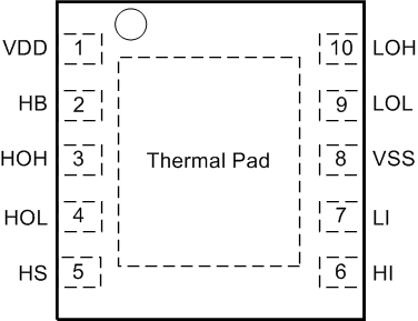
DPR Package
10-Pin WSON With Exposed Thermal Pad
Top View

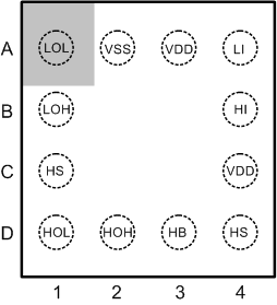
YFX Package
12-Pin DSBGA
Top View

Pin Functions
| PIN | TYPE (2) | DESCRIPTION | |||
|---|---|---|---|---|---|
| NAME | WSON | DSBGA | |||
| VDD | 1 | A3, C4(1) | P | 5-V Positive gate drive supply: locally decouple to VSS using low ESR/ESL capacitor located as close to the IC as possible. | |
| HB | 2 | D3 | P | High-side gate driver bootstrap rail: connect the positive terminal of the bootstrap capacitor to HB and the negative terminal to HS. The bootstrap capacitor should be placed as close to the IC as possible. | |
| HOH | 3 | D2 | O | High-side gate driver turnon output: connect to the gate of high-side GaN FET with a short, low inductance path. A gate resistor can be used to adjust the turnon speed. | |
| HOL | 4 | D1 | O | High-side gate driver turnoff output: connect to the gate of high-side GaN FET with a short, low inductance path. A gate resistor can be used to adjust the turnoff speed. | |
| HS | 5 | C1, D4(1) | P | High-side GaN FET source connection: connect to the bootstrap capacitor negative terminal and the source of the high-side GaN FET. | |
| HI | 6 | B4 | I | High-side driver control input. The LM5113 inputs have TTL type thresholds. Unused inputs should be tied to ground and not left open. | |
| LI | 7 | A4 | I | Low-side driver control input. The LM5113 inputs have TTL type thresholds. Unused inputs should be tied to ground and not left open. | |
| VSS | 8 | A2 | G | Ground return: all signals are referenced to this ground. | |
| LOL | 9 | A1 | O | Low-side gate driver sink-current output: connect to the gate of the low-side GaN FET with a short, low inductance path. A gate resistor can be used to adjust the turnoff speed. | |
| LOH | 10 | B1 | O | Low-side gate driver source-current output: connect to the gate of high-side GaN FET with a short, low inductance path. A gate resistor can be used to adjust the turnon speed. | |
| Exposed Pad | EP | — | — | Exposed pad: TI recommends that the exposed pad on the bottom of the package be soldered to ground plane on the printed-circuit board to aid thermal dissipation. | |
(1) A3 and C4, C1 and D4 are internally connected
(2) I = Input, O = Output, G = Ground, P = Power