JAJSDQ6C June 2012 – September 2017
PRODUCTION DATA.
- 1 特長
- 2 アプリケーション
- 3 概要
- 4 改訂履歴
- 5 Pin Configuration and Functions
-
6 Specifications
- 6.1 Absolute Maximum Ratings
- 6.2 ESD Ratings
- 6.3 Recommended Operating Conditions
- 6.4 Thermal Information
- 6.5 Electrical Characteristics: Front-End Amplification (Weight-Scale Signal Chain)
- 6.6 Electrical Characteristics: Body Composition Measurement Front-End
- 6.7 Electrical Characteristics: Analog-to-Digital Converter
- 6.8 Electrical Characteristics: Digital Input/Output
- 6.9 Timing Requirements: Serial Interface Timing
- 6.10 Typical Characteristics
-
7 Detailed Description
- 7.1 Overview
- 7.2 Functional Block Diagram
- 7.3 Feature Description
- 7.4 Device Functional Modes
- 7.5 Programming
- 7.6
Register Maps
- 7.6.1
Register Map
- 7.6.1.1 ADC_DATA_RESULT (Address 0x00, Default 0x0000)
- 7.6.1.2 ADC_CONTROL_REGISTER1 (Address 0x01, Default 0x01C3)
- 7.6.1.3 MISC_REGISTER1 (Address 0x02, Default 0x8000)
- 7.6.1.4 MISC_REGISTER2 (Address 0x03, Default 0x7FFF)
- 7.6.1.5 DEVICE_CONTROL1 (Address 0x09, Default 0x0000)
- 7.6.1.6 ISW_MUX (Address 0x0A, Default 0x0000)
- 7.6.1.7 VSENSE_MUX (Address 0x0B, Default 0x0000)
- 7.6.1.8 IQ_MODE_ENABLE (Address 0x0C, Default 0x0000)
- 7.6.1.9 WEIGHT_SCALE_CONTROL (Address 0x0D, Default 0x0000)
- 7.6.1.10 BCM_DAC_FREQ (Address 0x0E, Default 0x0000)
- 7.6.1.11 DEVICE_CONTROL2 (Address 0x0F, Default 0x0000)
- 7.6.1.12 ADC_CONTROL_REGISTER2 (Address 0x10, Default 0x0000)
- 7.6.1.13 MISC_REGISTER3 (Address 0x1A, Default 0x0000)
- 7.6.1
Register Map
- 8 Application and Implementation
- 9 Power Supply Recommendations
- 10Layout
- 11デバイスおよびドキュメントのサポート
- 12メカニカル、パッケージ、および注文情報
9 Power Supply Recommendations
9.1 Power-Supply Recommendation and Initialization
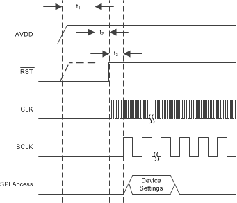
The device has an analog supply (AVDD). Drive these pins with a clean supply and connect bypass capacitors close to the pins. After power up, the device must be reset to set all internal registers to their default state. Resetting the device is done by applying an active low pulse on the RST pin after the power supplies stabilize. As part of the reset process, the AFE4300 sets all register bits to the respective default settings.
Some register bits must be written to values different from their default values after reset for proper operation. By default, the AFE4300 enters into a power-down state at start-up. The startup and initialization for the device is shown in Figure 16 and Table 6 lists the recommended timing values.
 Figure 16. Power-Up and Initialization
Table 6. Timing Parameters for Figure 16
| NOM | UNIT | ||
|---|---|---|---|
| t1 | Time between supplies turning on and an active RST | > 10 | ms |
| t2 | Active RST duration | > 50 | µs |
| t3 | Time between RST and register writes | > 1 | ms |