JAJSDQ6C June 2012 – September 2017
PRODUCTION DATA.
- 1 特長
- 2 アプリケーション
- 3 概要
- 4 改訂履歴
- 5 Pin Configuration and Functions
-
6 Specifications
- 6.1 Absolute Maximum Ratings
- 6.2 ESD Ratings
- 6.3 Recommended Operating Conditions
- 6.4 Thermal Information
- 6.5 Electrical Characteristics: Front-End Amplification (Weight-Scale Signal Chain)
- 6.6 Electrical Characteristics: Body Composition Measurement Front-End
- 6.7 Electrical Characteristics: Analog-to-Digital Converter
- 6.8 Electrical Characteristics: Digital Input/Output
- 6.9 Timing Requirements: Serial Interface Timing
- 6.10 Typical Characteristics
-
7 Detailed Description
- 7.1 Overview
- 7.2 Functional Block Diagram
- 7.3 Feature Description
- 7.4 Device Functional Modes
- 7.5 Programming
- 7.6
Register Maps
- 7.6.1
Register Map
- 7.6.1.1 ADC_DATA_RESULT (Address 0x00, Default 0x0000)
- 7.6.1.2 ADC_CONTROL_REGISTER1 (Address 0x01, Default 0x01C3)
- 7.6.1.3 MISC_REGISTER1 (Address 0x02, Default 0x8000)
- 7.6.1.4 MISC_REGISTER2 (Address 0x03, Default 0x7FFF)
- 7.6.1.5 DEVICE_CONTROL1 (Address 0x09, Default 0x0000)
- 7.6.1.6 ISW_MUX (Address 0x0A, Default 0x0000)
- 7.6.1.7 VSENSE_MUX (Address 0x0B, Default 0x0000)
- 7.6.1.8 IQ_MODE_ENABLE (Address 0x0C, Default 0x0000)
- 7.6.1.9 WEIGHT_SCALE_CONTROL (Address 0x0D, Default 0x0000)
- 7.6.1.10 BCM_DAC_FREQ (Address 0x0E, Default 0x0000)
- 7.6.1.11 DEVICE_CONTROL2 (Address 0x0F, Default 0x0000)
- 7.6.1.12 ADC_CONTROL_REGISTER2 (Address 0x10, Default 0x0000)
- 7.6.1.13 MISC_REGISTER3 (Address 0x1A, Default 0x0000)
- 7.6.1
Register Map
- 8 Application and Implementation
- 9 Power Supply Recommendations
- 10Layout
- 11デバイスおよびドキュメントのサポート
- 12メカニカル、パッケージ、および注文情報
6 Specifications
6.1 Absolute Maximum Ratings
over operating free-air temperature range (unless otherwise noted)(1)| MIN | MAX | UNIT | ||
|---|---|---|---|---|
| Voltage range | AVDD to AVSS | –0.3 | 4.1 | V |
| Any pin | –0.3 | AVDD + 0.3 | ||
| Diode current at any device pin | ±2 | mA | ||
| Maximum operating junction temperature, TJ max | 105 | °C | ||
| Storage humidity | 10% | 90% | Rh | |
| Storage temperature, Tstg | –25 | 85 | °C | |
(1) Stresses beyond those listed under Absolute Maximum Ratings may cause permanent damage to the device. These are stress ratings only, which do not imply functional operation of the device at these or any other conditions beyond those indicated under Recommended Operating Conditions. Exposure to absolute-maximum-rated conditions for extended periods may affect device reliability.
6.2 ESD Ratings
| VALUE | UNIT | |||
|---|---|---|---|---|
| V(ESD) | Electrostatic discharge | Human-body model (HBM), per ANSI/ESDA/JEDEC JS-001(1) | ±2000 | V |
| Charged-device model (CDM), per JEDEC specification JESD22-C101(2) | ±1000 | |||
(1) JEDEC document JEP155 states that 500-V HBM allows safe manufacturing with a standard ESD control process.
(2) JEDEC document JEP157 states that 250-V CDM allows safe manufacturing with a standard ESD control process.
6.3 Recommended Operating Conditions
over operating free-air temperature range (unless otherwise noted)| MIN | NOM | MAX | UNIT | |||
|---|---|---|---|---|---|---|
| AVDD | Supply voltage | 2 | 3.6 | V | ||
| AVSS | Ground | 0 | V | |||
| fCLK | External clock input frequency | 1 | MHz | |||
| TA | Ambient temperature range | 0 | 70 | °C | ||
6.4 Thermal Information
| THERMAL METRIC(1) | AFE4300 | UNIT | |
|---|---|---|---|
| PN (LQFP) | |||
| 80 PINS | |||
| RθJA | Junction-to-ambient thermal resistance | 50.5 | °C/W |
| RθJC(top) | Junction-to-case (top) thermal resistance | 14.2 | °C/W |
| RθJB | Junction-to-board thermal resistance | 25.3 | °C/W |
| ψJT | Junction-to-top characterization parameter | 0.5 | °C/W |
| ψJB | Junction-to-board characterization parameter | 24.9 | °C/W |
| RθJC(bot) | Junction-to-case (bottom) thermal resistance | N/A | °C/W |
(1) For more information about traditional and new thermal metrics, see the Semiconductor and IC Package Thermal Metrics application report.
6.5 Electrical Characteristics: Front-End Amplification (Weight-Scale Signal Chain)
over operating free-air temperature range, AVDD – AVSS = 3 V, G1 = 183, and G2 = 1 (unless otherwise noted)| PARAMETER | TEST CONDITIONS | AFE4300 | UNIT | ||||
|---|---|---|---|---|---|---|---|
| MIN | TYP | MAX | |||||
| BRIDGE SUPPLY | |||||||
| V(VLDO) | Output voltage (bridge supply voltage) | 1.7 | V | ||||
| IO | Output current | Current capability | 20 | mA | |||
| Short-circuit protection | 100 | mA | |||||
| tSTBY | Enable, disable time | With 470-nF capacitor on the VLDO pin | 1 | ms | |||
| AMPLIFICATION CHAIN | |||||||
| Offset error | With offset correction DAC disabled | 80 | µV | ||||
| Offset drift vs temperature | With offset correction DAC disabled | 0.25 | µV/°C | ||||
| Input bias current | ±70 | fA | |||||
| Input offset current | ±140 | fA | |||||
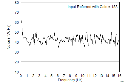
| Vn | Noise voltage, equivalent input | G1 = 183, 0.01 Hz < f < 2 Hz | 68 | nVrms | |||
| In | Noise current, equivalent input | f = 10 Hz | 100 | fA/√Hz | |||
| zid | Differential input impedance | 100 || 4 | GΩ || pF | ||||
| zic | Common-mode input impedance | 100 || 8 | GΩ || pF | ||||
| CMRR | Input common-mode rejection ratio | G1 = 183 | 95 | dB | |||
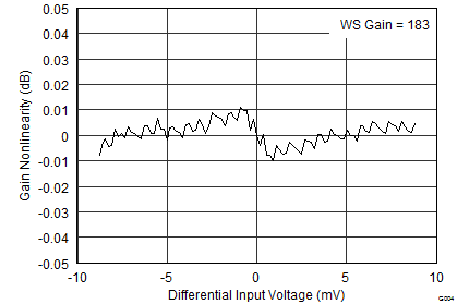
| INLWS | Gain nonlinearity | From input to digital output (including ADC) |
0.01 | % of FS(1) | |||
| First-stage gain equation | (1 + 2 × 100k / RG) | V/V | |||||
| tup | Power-up time | From power up to valid reading | 1 | ms | |||
| RFB1 | Internal feedback resistors | 95 | 100 | 105 | kΩ | ||
| Gain2 | Second-stage gain settings | 1, 2, 3, 4 | |||||
| Total gain error | ±5% | ||||||
| Offset DAC number of bits | 6 | Bits | |||||
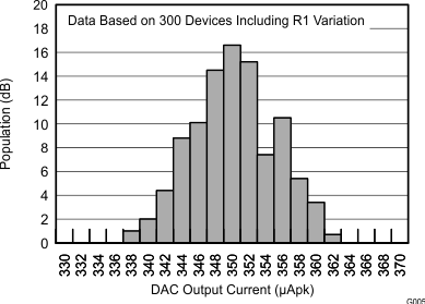
| IDAC | Full-scale offset DAC output current | ±6.5 | µA | ||||
(1) FS = full-scale.
6.6 Electrical Characteristics: Body Composition Measurement Front-End
over operating free-air temperature range, AVDD – AVSSS = 3 V (unless otherwise noted)6.7 Electrical Characteristics: Analog-to-Digital Converter
over operating free-air temperature range, AVDD – AVSS = 3 V (unless otherwise noted)| PARAMETER | TEST CONDITIONS | AFE4300 | UNIT | ||||
|---|---|---|---|---|---|---|---|
| MIN | TYP | MAX | |||||
| ANALOG-TO-DIGITAL CONVERTER | |||||||
| ADC input voltage range | At the input of the ADC (after PGA) | 2 × VREF | V | ||||
| VIN | Full-scale input voltage | At the input of the PGA | VADC / Gain | V | |||
| VREF | Reference voltage | 1.7 | V | ||||
| RON(mux) | Input multiplexer on-resistance | 0 V ≤ VAAUX ≤ AVDD | 6 | kΩ | |||
| AAUX input impedance | 4 | MΩ | |||||
| fDR | Output data rate | 8 | 860 | SPS | |||
| Resolution | 16 | Bits | |||||
| EI | Integral linearity error | Best fit, DR = 8 SPS | 1 | LSB | |||
| EO | Offset error | Differential inputs | ±1 | LSB | |||
| Single-ended inputs | ±3 | LSB | |||||
| EG | Gain error | 0.05% | |||||
| VBAT_MON | Battery monitor output | AVDD / 3 | V | ||||
| IBAT_MON | Battery monitor current consumption | 1.5 | µA | ||||
| IBAT_MON_ACC | Battery monitor accuracy | ±2% | |||||
| POWER CONSUMPTION | |||||||
| Supply current | Power-down current | 0.25 | µA | ||||
| Sleep-mode current | 100 | µA | |||||
| Weight-scale chain measurements | 540 | µA | |||||
| Body-composition measurements | 970 | µA | |||||
| Auxillary-channel measurements | 110 | µA | |||||
6.8 Electrical Characteristics: Digital Input/Output
over operating free-air temperature range, AVDD – AVSS = 3 V (unless otherwise noted)6.9 Timing Requirements: Serial Interface Timing
at TA = 0°C to +70°C and VDD = 2 V to 3.6 V (unless otherwise noted)| MIN | NOM | MAX | UNIT | ||
|---|---|---|---|---|---|
| tCSSC | STE low to first SCLK setup time(1) | 100 | ns | ||
| tSCLK | SCLK period | 250 | ns | ||
| tSPWH | SCLK pulse duration high | 100 | ns | ||
| tSPWL | SCLK pulse duration low | 100 | ns | ||
| tDIST | Valid SDIN to SCLK falling edge setup time | 50 | ns | ||
| tDIHD | Valid SDIN to SCLK falling edge hold time | 50 | ns | ||
| tDOPD | SCLK rising edge to valid new SDOUT propagation delay(2) | 50 | ns | ||
| tDOHD | SCLK rising edge to DOUT invalid hold time | 0 | ns | ||
| tCSDOD | STE low to SDOUT driven propagation delay | 100 | ns | ||
| tCSDOZ | STE high to SDOUT Hi-Z propagation delay | 100 | ns | ||
| tCSH | STE high pulse | 200 | ns | ||
| tSCCS | Final SCLK falling edge to STE high | 100 | ns | ||
(1) STE can be tied low.
(2) DOUT load = 20 pF || 100 kΩ to DGND.
 Figure 1. Serial Interface Timing


