JAJSEN3G March   2012  – March 2018 DRV110

PRODUCTION DATA.  

  1. 特長
  2. アプリケーション
  3. 概要
    1.     Device Images
      1.      電源ライン電圧によるDRV110への給電
  4. 改訂履歴
  5. Pin Configuration and Functions
    1.     Pin Functions
  6. Specifications
    1. 6.1 Absolute Maximum Ratings
    2. 6.2 ESD Ratings
    3. 6.3 Recommended Operating Conditions
    4. 6.4 Thermal Information
    5. 6.5 Electrical Characteristics
    6. 6.6 Typical Characteristics
  7. Detailed Description
    1. 7.1 Overview
    2. 7.2 Functional Block Diagram
    3. 7.3 Feature Description
      1. 7.3.1 Keep Time
      2. 7.3.2 PWM Current Control
      3. 7.3.3 Configuring Peak and Hold Currents
      4. 7.3.4 Configuring the PWM Frequency
      5. 7.3.5 Voltage Supply and Integrated Zener Diode
    4. 7.4 Device Functional Modes
      1. 7.4.1 Normal Mode
      2. 7.4.2 Shutdown
  8. Application and Implementation
    1. 8.1 Application Information
    2. 8.2 Typical Application
      1. 8.2.1 Design Requirements
      2. 8.2.2 Detailed Design Procedure
        1. 8.2.2.1 Current Limiting Resistor Selection
        2. 8.2.2.2 Passive Component Selection
      3. 8.2.3 Application Curve
  9. Power Supply Recommendations
  10. 10Layout
    1. 10.1 Layout Guidelines
    2. 10.2 Layout Example
  11. 11デバイスおよびドキュメントのサポート
    1. 11.1 ドキュメントのサポート
      1. 11.1.1 関連資料
    2. 11.2 ドキュメントの更新通知を受け取る方法
    3. 11.3 コミュニティ・リソース
    4. 11.4 商標
    5. 11.5 静電気放電に関する注意事項
    6. 11.6 Glossary
  12. 12メカニカル、パッケージ、および注文情報

Feature Description

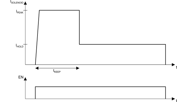
The DRV110 controls the current through the solenoid as shown in Figure 2. Activation starts when EN pin voltage is pulled high either by an external driver or internal pullup. In the beginning of activation, DRV110 allows the solenoid current to ramp up to the peak value IPEAK and it regulates it at the peak value for the time, tKEEP, before reducing it to IHOLD. The solenoid current is regulated at the hold value as long as the EN pin is kept high. The initial current ramp-up time depends on the inductance and resistance of the solenoid. Once EN pin is driven to GND, DRV110 allows the solenoid current to decay to zero.
DRV110 typ_current_wave_lvsba8.gifFigure 2. Typical Current Waveform Through the Solenoid