SBAU141A January 2009 – April 2024 PCM2912A
2.1 Pin Assignments and Terminal Functions
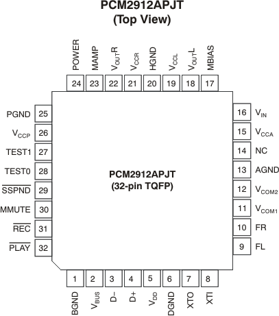
Figure 3-1 shows the pin assignments for the PCM2912A. Table 3-1 lists the terminal functions.
 Figure 2-1 PCM2912A
Pin Assignments
Figure 2-1 PCM2912A
Pin AssignmentsTable 2-1 PCM2912A Terminal
Functions
| Name | TQFP-36 Terminal |
I/O | Description |
|---|---|---|---|
| BGND | 1 | – | Reference for internal regulator |
| VBUS | 2 | – | Connect to USB power (VBUS) |
| D– | 3 | I/O | USB differential input/output minus |
| D+ | 4 | I/O | USB differential input/output plus |
| VDD | 5 | – | Digital power supply |
| DGND | 6 | Digital ground | |
| XTO | 7 | O | Crystal oscillator output |
| XTI | 8 | I | Crystal oscillator input |
| FL | 9 | – | External filter pin of left channel (optional) |
| FR | 10 | – | External filter pin of right channel (optional) |
| VCOM1 | 11 | – | Common voltage for ADC, DAC and analog front-end (VCCA/2). Decoupling capacitor is connected to AGND. |
| VCOM2 | 12 | – | Common voltage for headphone (VCCA/2). Decoupling capacitor is connected to AGND. |
| AGND | 13 | – | Analog ground |
| NC | 14 | – | Not connected |
| VCCA | 15 | – | Analog power supply |
| VIN | 16 | I | ADC microphone input |
| MBIAS | 17 | O | Microphone bias output (0.75 VCCA) |
| VOUTL | 18 | O | Headphone output for L-channel |
| VCCL | 19 | – | Analog power supply for headphone amplifier of L-channel |
| HGND | 20 | – | Analog ground for headphone amplifier |
| VCCR | 21 | -– | Analog power supply for headphone amplifier of R-channel |
| VOUTR | 22 | O | Headphone output for R-channel |
| MAMP | 23 | I | Microphone preamplifier gain control (LOW: Preamplifier off; HIGH: Preamplifier on = +20 dB) |
| POWER | 24 | I | Power consumption declaration select pin (LOW: 100 mA; HIGH: 500 mA) |
| PGND | 25 | – | Analog ground for microphone bias, microphone amplifier, and PGA |
| VCCP | 26 | – | Analog power supply for PLL |
| TEST1 | 27 | I | Test pin. Must be set to high. |
| TEST0 | 28 | I | Test pin. Must be set to low. |
| SSPND | 29 | O | Suspend flag (LOW: Suspend; HIGH: Operational state) |
| MMUTE | 30 | I | Microphone mute control, active high (LOW: Mute off; HIGH: Mute on) |
| REC | 31 | O | Status output for record (LOW: Record; FLASH: Mute on record; HIGH: Stop) |
| PLAY | 32 | O | Status output for playback (LOW: Playback; FLASH: Mute on playback; HIGH: Stop) |