SBAU269C October 2016 – August 2021 ADS8900B
2.3 Voltage Reference and VCM Scaling
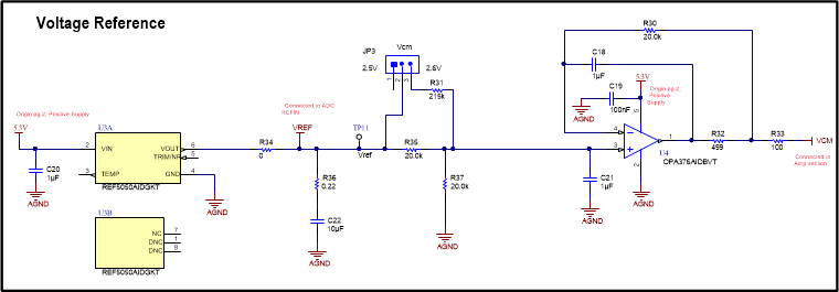
Figure 2-3 shows the voltage reference circuit, output filtering, voltage divider, and buffer
circuit. The REF5050 5-V, low-noise, low-drift voltage reference is used here. The
voltage reference is connected to the ADC directly to the right of R34 on the VREF node.
The filter R36 and C22 are selected for best noise performance and stability. As noted
in the REF5050 data sheet, the series resistor R36 is included to keep the capacitor ESR
in the desired range. The reference connects to a buffered input on the ADC so the
reference does not need to respond to transient current demands. The voltage divider
(R36, R31, and R37), and associated jumper (JP3) are used to set the common-mode input
for the FDA. The jumper provides the option of changing the common-mode input from 2.5 V
to 2.6 V. A common-mode of 2.5 V is midscale for a 0-V to 5-V FDA output swing. Because
of output swing limitations, some distortion may occur when the signal swings towards 0
V. The 2.6-V common-mode shifts the signal away from ground to avoid this distortion.
The theory behind this approach is documented in the Driving a SAR ADC with a Fully Differential Amplifier
video.
 Figure 2-3 Voltage Reference and VCM
Scaling
 Figure 2-3 Voltage Reference and VCM
Scaling