SBOU124B march   2012  – july 2023 INA230


  1.   1
  2.   INA230EVM Evaluation Board and Software Tutorial
  3.   Trademarks
  4. 1Overview
    1. 1.1 INA230EVM Kit Contents
    2. 1.2 Related Documentation from Texas Instruments
  5. 2INA230EVM Hardware
    1. 2.1 Theory of Operation for INA230 Hardware
    2. 2.2 Signal Definitions of H1 (10-Pin Connector Socket)
      1. 2.2.1 Theory of Operation for SM-USB-DIG Platform
  6. 3INA230EVM (Rev A) Hardware Setup
    1. 3.1 Electrostatic Discharge Warning
    2. 3.2 Connecting the Hardware
    3. 3.3 Connecting Power
    4. 3.4 Connecting the USB Cable to the SM-USB-DIG Platform
    5. 3.5 INA230EVM Default Jumper Settings
    6. 3.6 INA230EVM Features
      1. 3.6.1 J2: I2C VS Control Setting
      2. 3.6.2 J3 and J4: I2C Address Hardware Setting (A0)
      3. 3.6.3 J5 and J6: I2C Address Hardware Setting (A1)
      4. 3.6.4 External I2C Lines and Terminal Block T1
      5. 3.6.5 VIN+ and VIN– Input Filter (R1, R2, and C1)
      6. 3.6.6 Shunt Monitor Configuration and Terminal Blocks T3 and T4
  7. 4INA230EVM Software Setup
    1. 4.1 Operating Systems for the INA230EVM Software
    2. 4.2 Software Installation
  8. 5INA230EVM Software Overview
    1. 5.1 Starting the INA230EVM Software
    2. 5.2 Configuring the INA230EVM Software
      1. 5.2.1 I2C Address Selection
      2. 5.2.2 Configure Operating Mode
      3. 5.2.3 Set Conversion Times
      4. 5.2.4 Set Configuration Register
      5. 5.2.5 Configuring the Alert Pin
    3. 5.3 Using the INA230EVM Software
      1. 5.3.1 INA230 Bus Voltage, Shunt Voltage, Current, and Power Reading Bar
      2. 5.3.2 Calculation and Theory of Operation
      3. 5.3.3 Register Tab
      4. 5.3.4 Graph Tab
      5. 5.3.5 Auto-Write and the Supply Voltage
  9. 6INA230EVM Documentation
    1. 6.1 Schematic
    2. 6.2 PCB Layout
    3. 6.3 Bill of Materials
  10. 7Revision History

I2C Address Selection

The INA230 device has a flexible I2C address configuration that allows multiple devices on the same I2C lines. By moving the A0 and A1 addresses on jumpers J3-J6 to either GND, VS, SDA or SCL, the user can change the INA230 to a total of 16 I2C addresses (see Table 5-1).

Table 5-1 INA230 I2C Address Configuration
A1A0TARGET ADDRESS
GNDGND1000000
GNDVS+1000001
GNDSDA1000010
GNDSCL1000011
VS+GND1000100
VS+VS+1000101
VS+SDA1000110
VS+SCL1000111
SDAGND1001000
SDAVS+1001001
SDASDA1001010
SDASCL1001011
SCLGND1001100
SCLVS+1001101
SCLSDA1001110
SCLSCL1001111

Figure 5-3 shows how to configure the I2C addresses. Click the A0 or A1 box and select how to configure the hardware on the EVM. Failure to select the correct address prevents the INA230 device from communicating with the software.
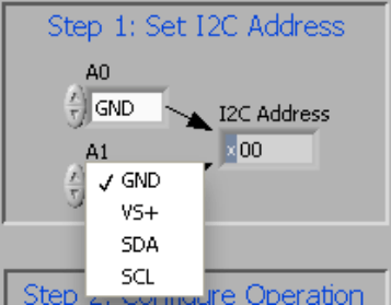
GUID-AAE7D803-37F6-4A14-A2E0-AD8830FE0657-low.gifFigure 5-3 Setting the A1 Address