SCAA124 April 2015 RM41L232 , RM42L432 , RM44L520 , RM44L920 , RM46L430 , RM46L440 , RM46L450 , RM46L830 , RM46L840 , RM46L850 , RM46L852 , RM48L530 , RM48L540 , RM48L730 , RM48L740 , RM48L940 , RM48L950 , RM48L952 , RM57L843 , TMS570LC4357 , TMS570LC4357-EP , TMS570LC4357-SEP , TMS570LS0232 , TMS570LS0332 , TMS570LS0432 , TMS570LS0714 , TMS570LS0714-S , TMS570LS0914 , TMS570LS1114 , TMS570LS1115 , TMS570LS1224 , TMS570LS1225 , TMS570LS1227 , TMS570LS2124 , TMS570LS2125 , TMS570LS2134 , TMS570LS2135 , TMS570LS3134 , TMS570LS3135 , TMS570LS3137
1.2 Latch-Up Model
Early in CMOS development, Latch-Up was recognized as a problem to be solved. Research and development into the causes led to several papers in the 1980’s discussing causes and methods to lessen the influence of Latch-Up. The NMOS and PMOS circuits form parasitic PNPN structures that can be triggered when a current or voltage impulse is directed into an input, output or power supply.
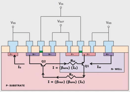
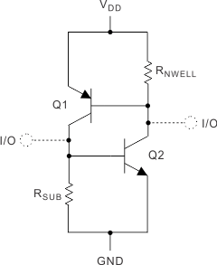
Figure 1 shows a typical, simple, cross-section of a CMOS inverter in an N-Well, P- substrate, CMOS process. The PMOS forms a parasitic vertical PNP from the P+ source/drain of the transistor (emitter), the N-Well (base) and the substrate (collector). A lateral NPN is formed from the N+ source/drain (emitter), P- substrate (base) and the N-Well (collector). The resultant circuit describes a PNPN (as shown in Figure 2).
As an example, if a current impulse strikes the PMOS drain, the P+/ N-Well junction (Q1) becomes forward biased. If the impulse is high enough (sustainable for a sufficient length of time), the carriers injected into the substrate cause a voltage drop across the substrate resistance. The bias across the P- / N+ (substrate to NMOS drain) in Q2 is then high enough to turn-on Q2. The Q2 collector current will then flow into the base of Q1. At that time, the Latch-Up becomes self-sustaining, a positive feedback loop has been formed. Only cessation of the power supply can stop the Latch-Up condition.
Temperature effects (external and internal to the product) can also influence the Latch-Up immunity of products. As temperature increases, the substrate and well resistances rise allowing the bias to reach a critical value sooner. Also, the effective distance between the N+, P+ and N-Well diffusions narrows allowing easier capture of excited carriers.
 Figure 1. Cross-Section of a CMOS Inverter
  Figure 2. Lateral NPN