SLAA502A July 2011 – September 2023 MSP430FR5720 , MSP430FR5721 , MSP430FR5722 , MSP430FR5723 , MSP430FR5724 , MSP430FR5725 , MSP430FR5726 , MSP430FR5727 , MSP430FR5728 , MSP430FR5729 , MSP430FR5730 , MSP430FR5731 , MSP430FR5732 , MSP430FR5733 , MSP430FR5734 , MSP430FR5735 , MSP430FR5736 , MSP430FR5737 , MSP430FR5738 , MSP430FR5739
5 MSP430FR57xx Family
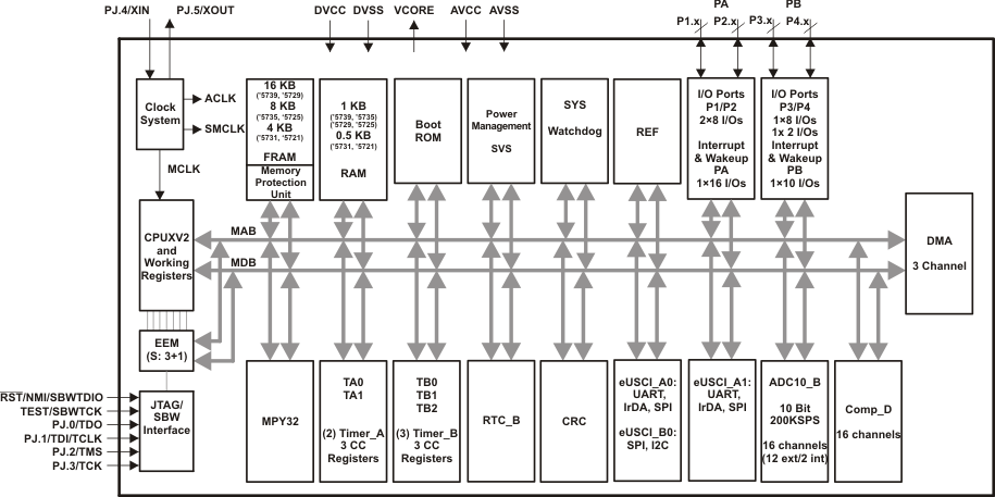
Beyond integrating FRAM as their main memory technology, the MSP430FR57xx family of devices have other unique features such as an extremely low active mode current consumption of ~100 µA/MHz. They also offer a rich mixture of peripherals including communication ports, timers, and a 10-bit ADC with integrated reference (see the block diagram in Figure 5-1).
The MSP430FR57xx family offers 20 different devices with FRAM memories up to 16 kB. The devices are offered in four packages ranging from a tiny 24-pin QFN to a 40-pin QFN, as well as 28-pin and 38-pin TSSOP packages. See the MSP430FR57xx data sheet for more information.
 Figure 5-1 MSP430FR57xx Family Block Diagram