SLAAEE6 October 2023 MSPM0L1306 , MSPM0L1306
8.3 Runtime Calibration
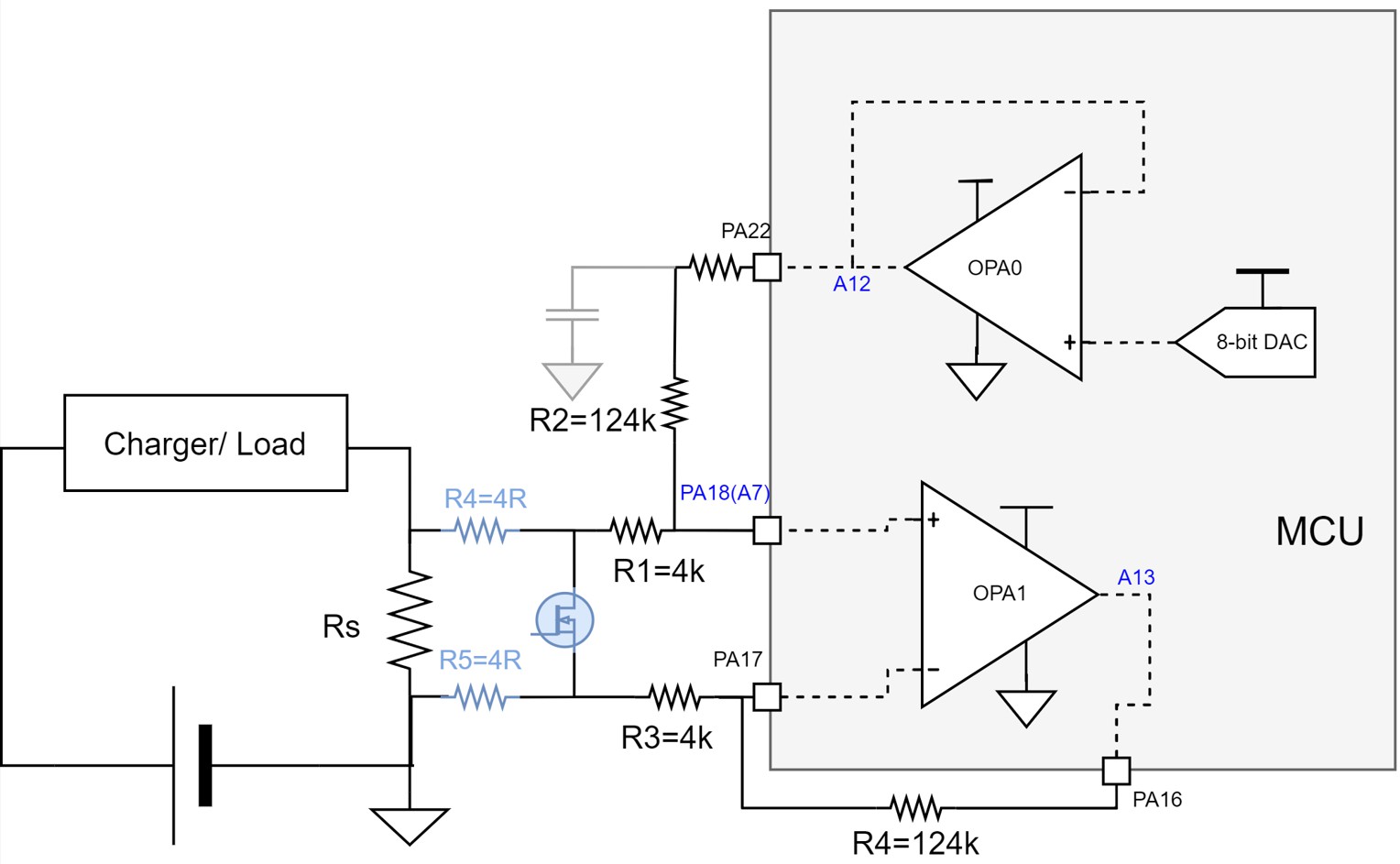
As this demo will only do calibration at first power up, if the temperature changes, the GAIN factor and Voffset are also influenced. If you want to realize runtime calibration, the power-on current cannot be 0, especially for the MCU on system side. The structure in Figure 8-1 can be used.
 Figure 8-1 Runtime Calibration Hardware Structure
In this structure, during calibration, the MOSFET should be enabled. The current across Rs are divided by R4 and R5, which are treated as the common voltage input into the amplifier. From Equation 5, you know that the mismatch between R1, R2, R3 and R4 causes the common voltage to have a large influence on the OPA output. So, you should make sure that R2=R4 and R3=R1. As internal gain has larger gain error (2.7% with GAIN32), use external gain instead.
For Voffset calibration, it can use the Voffset calibrated with internal gain to simulate the real Voffset. For R3/(R3+R4) calibration, it can be done by detection the voltage on ADC channel 7 and ADC channel 13. For (R1+R2)/R2 calibration, you can use a default value at the beginning and do the calibration when the load current is low and the error influence can be ignored. It is not suggested that you use another ADC to detect the voltage across Rs in the calibration to make up the error cause from the load current. First, is that this detection voltage will be positive only when in discharge mode. Second, the tested result is affected by ADC offset error.