SLAU546A March 2014 – October 2021 TRF37A73 , TRF37A75 , TRF37B73 , TRF37B75 , TRF37C73 , TRF37C75 , TRF37D73
4 EVM Board Loss
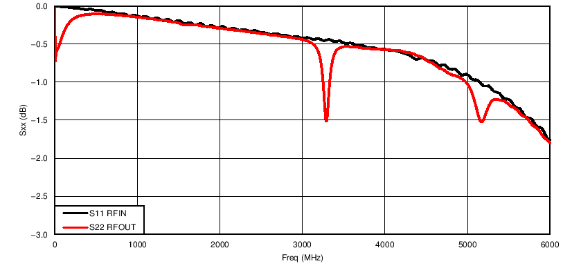
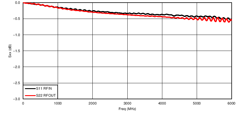
Performance plots of the TRF37x73/75 EVM board are illustrated in Figure 4-1 and Figure 4-2, with the following modifications to the BOM:
- U1 gain block uninstalled
- C1 and C2 removed, terminals shorted with strip of copper whose width equaled the trace width.
Figure 4-1 and Figure 4-2 show the S11 and S22 log magnitude responses to a –10-dBm input signal. These measurements were taken with an Agilent E5071B vector network analyzer calibrated from 1 MHz to 6 GHz to the end of the coaxial cables. The coaxial cables were connected directly to J1 and J2 on the EVM board. Port 1 refers to J1 in the schematic and Port 2 refers to J2 in the schematic.
 Figure 4-1 S11, S22 (Open), U1 Uninstalled
 Figure 4-2 S11, S22 (Open), U1 and L1 Uninstalled, Copper Tape Replaced C1 and C2