SLAU546A March 2014 – October 2021 TRF37A73 , TRF37A75 , TRF37B73 , TRF37B75 , TRF37C73 , TRF37C75 , TRF37D73
5.3 OIP3
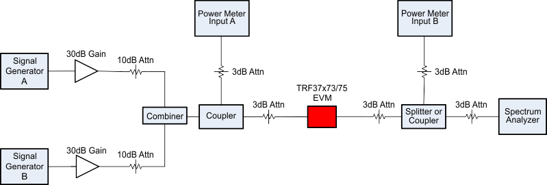
Recommendations and comments:
- This setup can also be used for gain and P1dB, if desired
- For wideband measurements, the 30-dB gain stage and 10-dB attenuators are used to improve the input IP3 level that is created from the interaction of the 2 signal generators via the isolation of the combiner. For narrow band measurements, it maybe possible to create a setup with enough isolation using an isolator and/or combiner. In this case the 10-dB pads could be reduced or removed.
- Power meter A is used to ensure the amplitude of the two tones at the input of the TRF37x73/75 EVM are within a certain tolerance. The gain stages will have unique gain characteristics and their gain can drift over time
- Power meter B can be used for measuring the amplitude of individual tones for more accurate measurements.
- Keep spectrum analyzer RBW and VBW settings identical for main tone and IM3 products
- Take into account losses of coax and attenuators to and from the EVM board
- Take into account losses of traces on the board up to the I/O pins of the DUT