SLAU678C March   2016  – November 2022


  1.   Abstract
  2.   Trademarks
  3. 1Getting Started
    1. 1.1 Introduction
    2. 1.2 Key Features
    3. 1.3 What's Included
      1. 1.3.1 Kit Contents
      2. 1.3.2 Software Examples
    4. 1.4 First Steps: Out-of-Box Experience
      1. 1.4.1 Connecting to the Computer
      2. 1.4.2 Running the Out-of-Box Demo
        1. 1.4.2.1 Live Temperature Mode
        2. 1.4.2.2 FRAM Data Log Mode
        3. 1.4.2.3 SD Card Data Log Mode
    5. 1.5 Next Steps: Looking Into the Provided Code
  4. 2Hardware
    1. 2.1 Block Diagram
    2. 2.2 Hardware Features
      1. 2.2.1 MSP430FR5994 MCU
      2. 2.2.2 eZ-FET Onboard Debug Probe With EnergyTrace++ Technology
      3. 2.2.3 Debug Probe Connection: Isolation Jumper Block
      4. 2.2.4 Application (or Backchannel) UART
      5. 2.2.5 Special Features
        1. 2.2.5.1 microSD Card
        2. 2.2.5.2 220-mF Super Capacitor
    3. 2.3 Power
      1. 2.3.1 eZ-FET USB Power
      2. 2.3.2 BoosterPack Plug-in Module and External Power Supply
      3. 2.3.3 Super Cap (C1)
        1. 2.3.3.1 Charging the Super Cap
        2. 2.3.3.2 Using the Super Cap
        3. 2.3.3.3 Disabling the Super Cap
    4. 2.4 Measure MSP430 Current Draw
    5. 2.5 Clocking
    6. 2.6 Using the eZ-FET Debug Probe With a Different Target
    7. 2.7 BoosterPack Plug-in Module Pinout
    8. 2.8 Design Files
      1. 2.8.1 Hardware
      2. 2.8.2 Software
    9. 2.9 Hardware Change Log
  5. 3Software Examples
    1. 3.1 Out-of-Box Software Example
      1. 3.1.1 Source File Structure
      2. 3.1.2 Out-of-Box Demo GUI
      3. 3.1.3 Power Up and Idle
      4. 3.1.4 Live Temperature Mode
      5. 3.1.5 FRAM Log Mode
      6. 3.1.6 SD Card Log Mode
    2. 3.2 Blink LED Example
      1. 3.2.1 Source File Structure
    3. 3.3 BOOSTXL-AUDIO Audio Record and Playback Example
      1. 3.3.1 Source File Structure
      2. 3.3.2 Operation
    4. 3.4 Filtering and Signal Processing With LEA Reference Design Example
      1. 3.4.1 Source File Structure
      2. 3.4.2 Operation
    5. 3.5 Emulating EEPROM Reference Design Example
      1. 3.5.1 Source File Structure
      2. 3.5.2 Operation
  6. 4Resources
    1. 4.1 Integrated Development Environments
      1. 4.1.1 TI Cloud Development Tools
        1. 4.1.1.1 TI Resource Explorer Cloud
        2. 4.1.1.2 Code Composer Studio Cloud
      2. 4.1.2 Code Composer Studio™ IDE
      3. 4.1.3 IAR Embedded Workbench for MSP430
    2. 4.2 LaunchPad Websites
    3. 4.3 MSPWare and TI Resource Explorer
    4. 4.4 FRAM Utilities
      1. 4.4.1 Compute Through Power Loss (CTPL)
    5. 4.5 MSP430FR5994 MCU
      1. 4.5.1 Device Documentation
      2. 4.5.2 MSP430FR5994 Code Examples
      3. 4.5.3 MSP430 Application Notes and TI Reference Designs
    6. 4.6 Community Resources
      1. 4.6.1 TI E2E Support Forums
      2. 4.6.2 Community at Large
  7. 5FAQ
  8. 6Schematics
  9. 7Revision History

Debug Probe Connection: Isolation Jumper Block

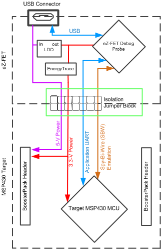
The isolation jumper block at jumper J101 can connect or disconnect signals that cross from the eZ-FET domain into the MSP430FR5994 target domain. This includes eZ-FET Spy-Bi-Wire signals, application UART signals, and 3.3-V and 5-V power (see Table 2-2 and Figure 2-5).

Reasons to open these connections:

  • To remove any and all influence from the eZ-FET debug probe for high accuracy target power measurements
  • To control 3-V and 5-V power flow between the eZ-FET and target domains
  • To expose the target MCU pins for other use than onboard debugging and application UART communication
  • To expose the programming and UART interface of the eZ-FET so that it can be used for devices other than the onboard MCU.
Table 2-2 Isolation Block Connections
JumperDescription
GNDGround
5V5-V VBUS from USB
3V33.3-V rail, derived from VBUS in the eZ-FET domain
RXD <<Backchannel UART: The target MSP430FR5994 receives data through this signal. The arrows indicate the direction of the signal.
TXD >>Backchannel UART: The target MSP430FR5994 sends data through this signal. The arrows indicate the direction of the signal.
SBW RSTSpy-Bi-Wire debug: SBWTDIO data signal. This pin also functions as the RST signal (active low).
SBW TSTSpy-Bi-Wire debug: SBWTCK clock signal. This pin also functions as the TST signal.
GUID-CAC49203-CFAB-4DE5-BA65-04ADBC216276-low.gifFigure 2-5 eZ-FET Isolation Jumper Block Diagram