SLDU019B December   2015  – March 2016 PGA450-Q1


  1.   PGA450Q1EVM-S User's Guide and TIDA-00151 UART Demo Instructional
    1.     Trademarks
    2. 1 Introduction
    3. 2 Setup and Operation
      1. 2.1 Input and Output Connectors
      2. 2.2 Basic Operation
        1. 2.2.1 Programming the PGA450-Q1 DEVRAM or OTP Memory
        2. 2.2.2 Programming the PGA450-Q1 EEPROM
        3. 2.2.3 Testing the UART Connection With the TI GER Board
      3. 2.3 UART Command Listing
    4. 3 Software
      1. 3.1 IDE Output File Configuration
        1. 3.1.1 Setup for DEVRAM Output File
        2. 3.1.2 Setup for OTP Output File
      2. 3.2 Interface Descriptions
        1. 3.2.1 UART Interface
        2. 3.2.2 LIN Interface
        3. 3.2.3 Serial-Peripheral Interface
    5. 4 Schematic, Bill of Materials, and Layout
      1. 4.1 Schematic
      2. 4.2 Bill of Materials
        1. 4.2.1 BOM
      3. 4.3 Board Layout and Component Placement
    6. 5 References
  2.   Revision History

Board Layout and Component Placement

Figure 9 and Figure 10 show the top and bottom views component placement. Figure 11 and Figure 12 show the top and bottom views of the board layout.
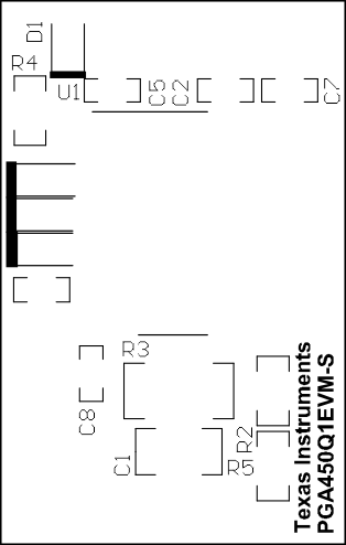
layer_top_overview_sldu019.gifFigure 9. Component Placement – Top Overview
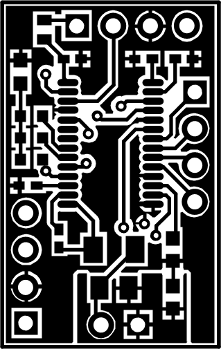
layer_top_sldu019.gifFigure 11. Layout – Top
layer_bottom_overview_sldu019.gifFigure 10. Component Placement – Bottom Overview
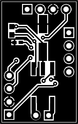
layer_bottom_sldu019.gifFigure 12. Layout – Bottom