SLUAAL2 june 2023 UCC256402 , UCC256403 , UCC256404
- 1
- Abstract
- Trademarks
-
1UCC25640x Frequently Asked Questions
- 1.1 For the Time Domain Simulation and Fundamental Harmonic Analysis of LLC Resonant Converters, What Model of the Transformer Should be Used?
- 1.2 How to Connect External Gate Drivers to the UCC25640x for High Gate Driver Current Capability?
- 1.3 When Powering on the PFC-LLC AC-DC Converter, What Sequence is Recommended?
- 1.4 How to Eliminate the Nuisance ZCS Detection During the Light Load?
- 1.5 What is the Purpose of Maintaining the FB Pin Voltage of the UCC25640x Controllers at a Constant Level?
- 1.6 How to Improve the Slew Rate Detection at HS Pin of the UCC25640x Controller?
- 1.7 How to Operate the UCC25640x Controller in the Open Loop?
- 1.8 What Happens if the VCR Pin Peak to Peak Voltage of the Controller Exceeds 6 V?
- 1.9 What UCC25640x settings effect the startup duration of the LLC?
- 1.10 What is Causing the Current Imbalance in the LLC's Secondary Side Windings?
- 1.11 How to Design TL431 Compensator for LLC With UCC25640x Controller
- 1.12 How to Design LLC for Battery Charging and LED Driver Applications?
- 1.13 How to Implement CC-CV Feedback Control?
- 1.14 What is the Simplest Approach to Configure the Burst Mode Thresholds for UCC25640x Based on the Load Power?
- 1.15 How to Avoid the UCC25640x Controller to Enter into Burst Mode?
- 1.16 What are the Methods for Preventing VCC From Decreasing Below the VCC Restart Threshold During Burst Mode?
- 1.17 How Does BMTL Threshold Value Impacts the Output Voltage Ripple and the VCC Pin Voltage and Magnetizing Current?
- 1.18 How to Design Magnetics for LLC?
- 1.19 How is the Dead Time in UCC25640x Determined During ZCS Detection and in the Absence of Valid Slew Rate Detection?
- 2References
1.6 How to Improve the Slew Rate Detection at HS Pin of the UCC25640x Controller?
UCC25640x has a minimum detectable slew rate of 100 mV/ns. As soon as the high side gate (HO) is turned off, the low side gate (LO) is be turned on after the slew rate has been detected. If the slew rate detection is missed, the dead time depends on the resonant current polarity (Section 1.19). Figure 1-10 shows a way of extracting slew rate information during the dead time [10]. In this simulation Infineon IPW6075CP MOSFET is used as an example. Figure 1-11 shows the switch node voltage transition when a current of 0.7 A is being pulled out from switch node. Here we can observe that switch node voltage has different slew rates during the transition which is due to non linear capacitance (Figure 1-15) seen at the switch node. This non linear capacitance is combination of Coss of the both upper (voltage changing from 0 V to 390 V) and lower (voltage changing from 390 V to 0 V) MOSFETs as shown in Figure 1-13 and Figure 1-14. The Coss graphs of each MOSFETs are extracted using the SIMetrix simulation. The extractions are shown in Figure 1-12.
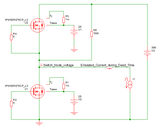 Figure 1-10 SIMetrix
Simulation for Finding Switch Node Slew Rate During Dead Time
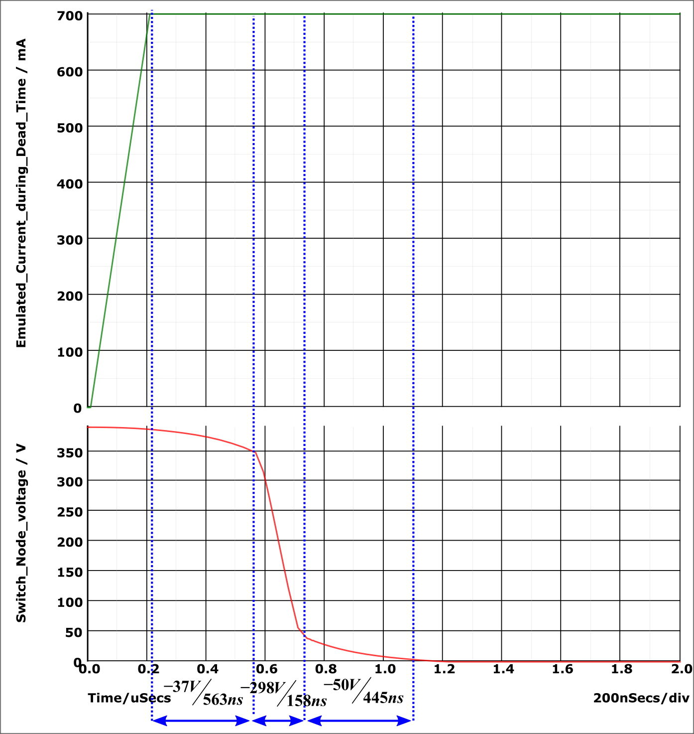 Figure 1-11 Switch
Node Voltage Slew Rates During Dead Time
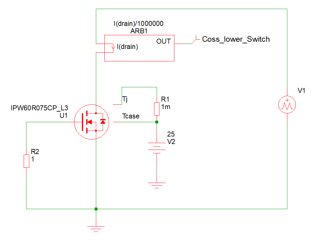 Figure 1-12 Coss
Extraction From Device Model Using SIMetrix
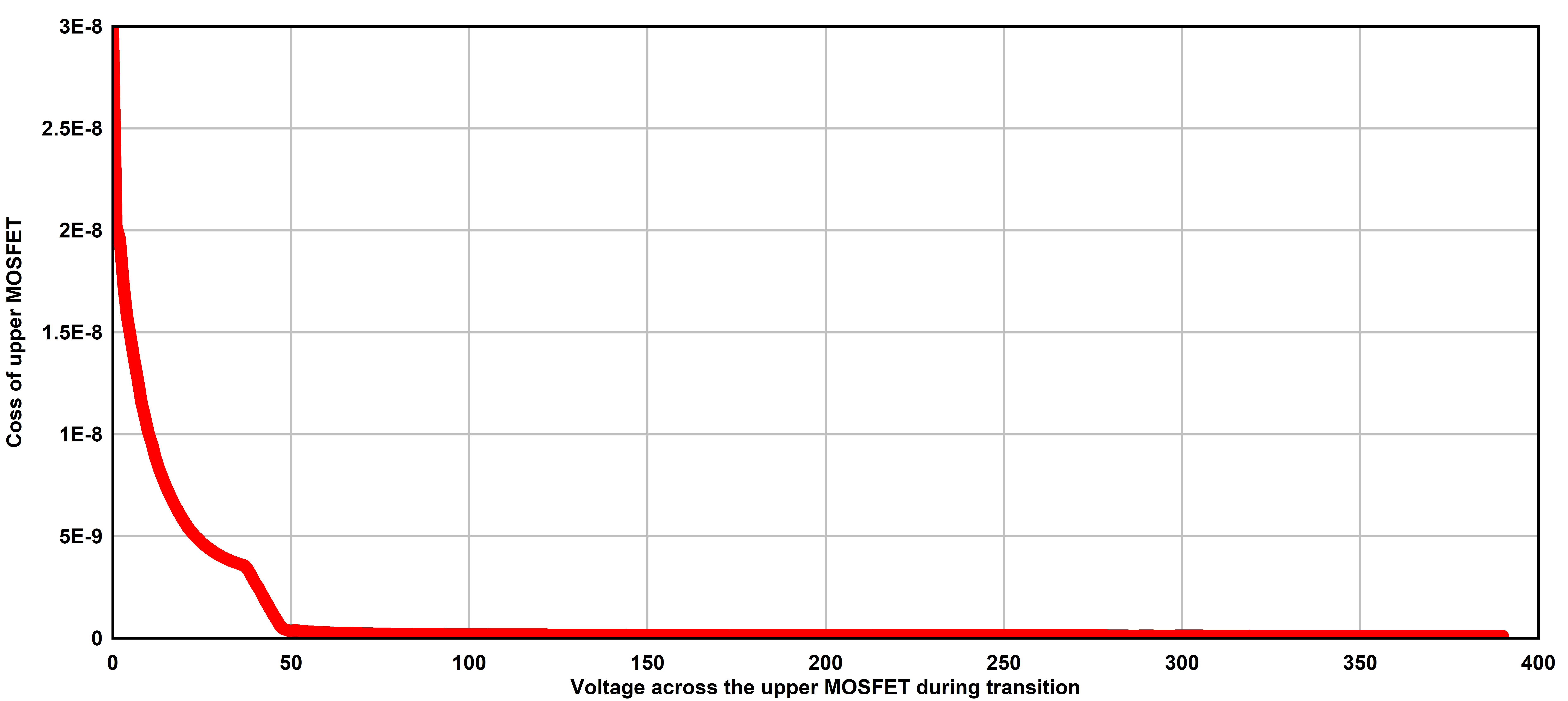 Figure 1-13 Upper
MOSFETs Coss vs Drain to Source Voltage
 Figure 1-15 Coss
Seen at the Switch Node vs Switch Node Voltage
 Figure 1-14 Lower
MOSFETs Coss vs Drain to Source Voltage
Figure 1-14 Lower
MOSFETs Coss vs Drain to Source VoltageThe following methods can be followed to improve the slew rate detection:
- Increase the MOSFET turn off speed: Most designs include a diode in the HO/LO gate drive paths to allow for independent turn on and turn off speed. Such a circuit is recommended to increase the turn off speed of the gate drive.
- Using MOSFETs with lower output capacitance (Coss): The lower Coss allow for a faster switch node slew rate.
- Using a higher burst mode setting: A higher burst mode setting have larger magnetizing current amplitude which help with achieving the dV/dt criteria (Increasing the burst threshold make the LLC burst with slightly more power within the burst packet and the resonant current amplitude can be higher.
- Reducing any snubber capacitance on the switch node
- Reducing the magnetizing inductance of the transformer to increase the magnetizing current at light load.