SLVA680A February 2015 – April 2022 ESD401 , TPD12S015 , TPD12S015A , TPD12S016 , TPD12S520 , TPD12S521 , TPD13S523 , TPD1E05U06 , TPD1E10B06 , TPD1E10B09 , TPD1S414 , TPD1S514 , TPD2E001 , TPD2E001-Q1 , TPD2E009 , TPD2E1B06 , TPD2E2U06-Q1 , TPD2EUSB30 , TPD2S017 , TPD3S014 , TPD3S044 , TPD4E001-Q1 , TPD4E004 , TPD4E02B04 , TPD4E05U06 , TPD4E05U06-Q1 , TPD4E101 , TPD4E1U06 , TPD4E6B06 , TPD4EUSB30 , TPD4S010 , TPD4S014 , TPD4S1394 , TPD4S214 , TPD5S115 , TPD5S116 , TPD6E004 , TPD6E05U06 , TPD6F002-Q1 , TPD6F003 , TPD7S019 , TPD8E003 , TPD8F003
1 Introduction
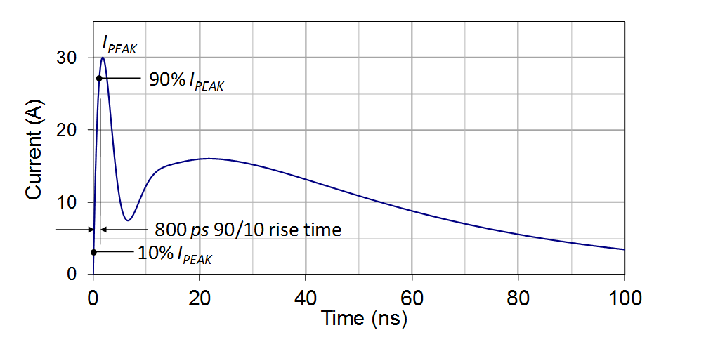
An ESD event rapidly forces current (see Figure 1-1), IESD , into a system, usually through a user interface such as a cable connection, or a human input device like a key on a keyboard. Protecting a system against ESD using a TVS relies upon the TVS being able to shunt IESD to ground. Optimizing a PCB Layout for ESD suppression is largely dependant on designing the path to ground for IESD with as little impedance as possible. During an ESD event, the voltage presented to the protected integrated circuit (Protected IC), VESD, is a function of IESD and the impedance presented to it. Since the designer has no control over IESD, lowering the impedance to ground is the primary means available for minimizing VESD.
Lowering the impedance presents several challenges. Mainly, it cannot be of zero impedance, or the signal line being protected would be shorted to ground. In order for the circuit to have a realistic application, the protected line needs to be able to maintain some voltage, usually under a high impedance to ground. This is where the TVS becomes applicableLowering the impedance presents several challenges. Mainly, it cannot be of zero impedance, or the signal line being protected would be shorted to ground. In order for the circuit to have a realistic application, the protected line needs to be able to maintain some voltage, usually under a high impedance to ground. This is where the TVS becomes applicable Figure 1-1 IEC
61000-4-2 Compliant Level 4 (8 kV ESD) Waveform
Figure 1-1 IEC
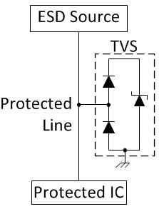
61000-4-2 Compliant Level 4 (8 kV ESD) WaveformA TVS is an array of diodes (see Figure 1-2 for a typical example) arranged to present a very high impedance to the voltages normally present in the circuit, but if voltages exceed the design, the TVS diodes will breakdown and shunt IESD to ground before it can damage the system being protected. The system designer is then challenged to lower the impedance for IESD from the ESD Source through the TVS to ground.
 Figure 1-2 A Typical
ESD Protection Scheme
Figure 1-2 A Typical
ESD Protection SchemeThe impedance presented to IESD is a function of any impedance inherent with the TVS (in the diode array and the package of the TVS) and the PCB Layout between the ESD Source and the TVS ground. A TVS is generally designed to offer as low of an impedance to ground for IESD as its overall design constraints will allow. With the proper TVS selected, a critical phase of the design is to lower the impedance in the PCB Layout between the ESD Source and the TVS ground.
Another concern created by the rapidly changing IESD is its associated rapidly changing electromagnetic field (EM) causing interference (EMI) to couple onto other circuits of the PCB. This is especially true in the area between the ESD Source and the TVS. Once the TVS shunts IESD to ground, the trace between the TVS and the Protected IC should be relatively free of EMI. Therefore, unprotected circuits should not be adjacent to an ESD protected circuit's traces between the ESD Source and the TVS. In order to keep EMI emissions at a minimum, circuit traces between the ESD Source and the TVS should have corners which do not exceed 45° or, ideally, which are curved with large radii.
In today's PCB Layout, board space is at a premium. ICs, including TVSs, are designed to be very compact. Also, the density of their placement on the PCB is continually increasing. Multiple layer PCB boards and routing lean heavily upon VIAs for maximizing the density to increase the system's feature set while decreasing the system's size. This PCB architecture, particularly related to layer switching and VIAs, plays an important role in shunting IESD to ground through the TVS. Large differences in VESD at the Protected IC can be induced by the manner in which the circuit is routed to the TVS using VIAs. Generally, placing a VIA between the ESD Source and the TVS is detrimental, but in some circumstances the designer is forced to do so. Even in these circumstance, if properly done, VESD can still be minimized at the Protected IC.
Grounding schemes are critical in protecting against ESD. Having a chassis ground for the TVS that is separated from the digital and/or analog ground by inductance provides very good protection against ESD related failures. Yet it presents great challenges when routing high speed circuits across multiple ground planes. For this reason, many designs use one common ground for the protected circuits. Ground planes are necessary for the TVS to have success in dissipating IESD without increasing VESD. Electrical connections to an earth grounded chassis, like a PCB grounded through-hole for a chassis screw, immediately adjacent to the TVS ground and the ESD Source's ground (for example, a connector shield) provide a sound methodology in keeping ground shifts at Protected ICs to a minimum. If a system cannot utilize a chassis earth ground, tightly coupled multiple layer ground planes can help keep ground shifts at Protected ICs to a minimum.
To summarize these parameters, successfully protecting a system against ESD includes:
- Controlling impedances around the TVS for dissipating ESD current, IESD
- Limiting the effects of EMI on unprotected circuits
- Properly using VIAs to maximize ESD dissipation by the TVS
- Designing a grounding scheme which has very low impedance for the TVS