SLVAEJ0 April 2020 TPS25830-Q1 , TPS25830A-Q1 , TPS25831-Q1 , TPS25832-Q1 , TPS25833-Q1 , TPS25840-Q1 , TPS25842-Q1 , TPS25846-Q1
2 Data Communication Issue Caused by Ground Shift
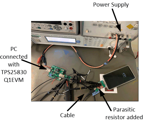
In order to validate the ground shift influence for USB data communication, the bench shown in Figure 2 was built.
 Figure 2. Bench Setup for Ground Shift Test
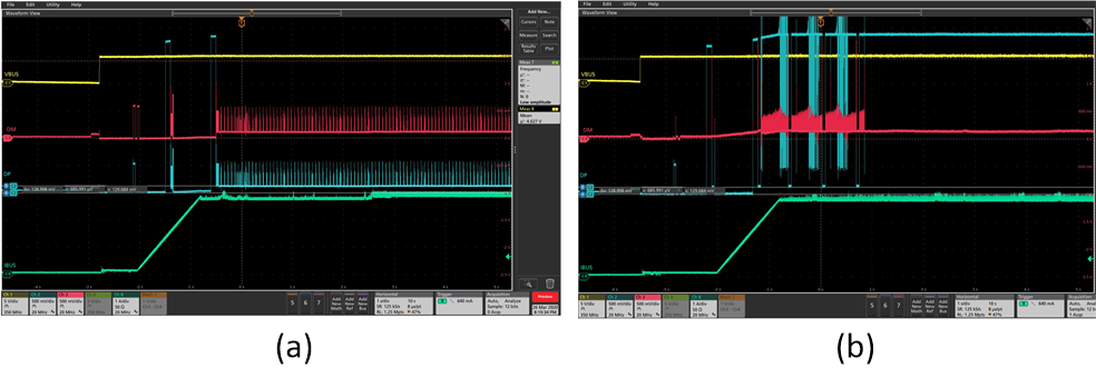
 Figure 3 shows the data communication and charging waveforms without additional resistor added.
- Condition:
- Results:
In CDP mode, without cable compensation, pixel2 phone, and parasitic resistor not added, only USB cable and connector wire.
With secondary detection finished (CDP mode), enumeration starts and also the phone draws current. With a process of recognition from full speed to the high speed signal, data communication starts successful. The ground voltage shift is about 129 mV. Voltage at the terminal of IC is about 5 V . Current draw by the phone is about 3A.
Per the USB2.0 spec, the maximum voltage drop for all cables between upstream and downstream on GND is 125 mV. Although the data communication is normal, after you plug and unplug the phone several times, the phone data communication fails., see Figure 3.
 Figure 3. (a) Without Additional Resistor Added (b) Without Additional Resistor Added but Pug and Unplug Phone Several Times
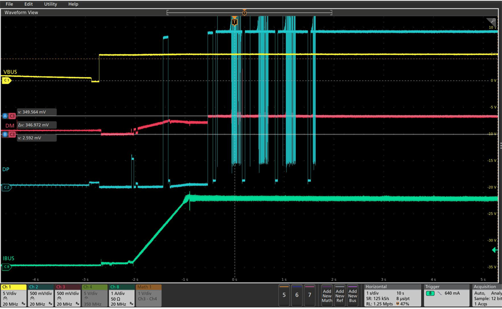
 Figure 4 shows related waveforms with parasitic resistor added.
- Condition:
- Results:
In CDP mode, without cable compensation, pixel2 phone, and 20 mΩ parasitic resistor added on ground line.
The ground voltage shift is about 347 mV. The data signal voltage is about 400 mV + 347 mV = 747 mV, which is far out of the range of 625 mV. Current drawing is about 2.6A due to VBUS voltage drop. Data communication also fails. As shown in Figure 4, too high parasitic resistor on the ground line leads to too high ground voltage shift, which will boost the data signal voltage out of threshold causing data communication failure and VBUS drops with low charging current.
 Figure 4. Charging and Data Communication Waveforms With Parasitic Resistor Added