SLVAEJ0 April 2020 TPS25830-Q1 , TPS25830A-Q1 , TPS25831-Q1 , TPS25832-Q1 , TPS25833-Q1 , TPS25840-Q1 , TPS25842-Q1 , TPS25846-Q1
4 Suggestions for Ground Shift Issue
- Shorten and widen the ground trace as layout to reduce the parasitic resistor.
- Use standard USB cable that has lower parasitic resistor than non-standard USB cable.
- Use chips with cable compensation function for high charging current such as TPS2583x-Q1.
- Better to have single point GND connection, not only beneficial to ground shift issue but also to reduce ground bounce issue.
- Increasing the host side voltage level is as well one optional method to solve ground shift issue.
- USB interface contact resistance is also one big influence factor which leads to ground shift. The contact resistance is relatively high. It is suggested to adopt USB terminal with low contact resistance. Widen the contact trace is also beneficial to reduce the contact resistance.
- There are two ways to identify whether it’s the ground shift issue or not.
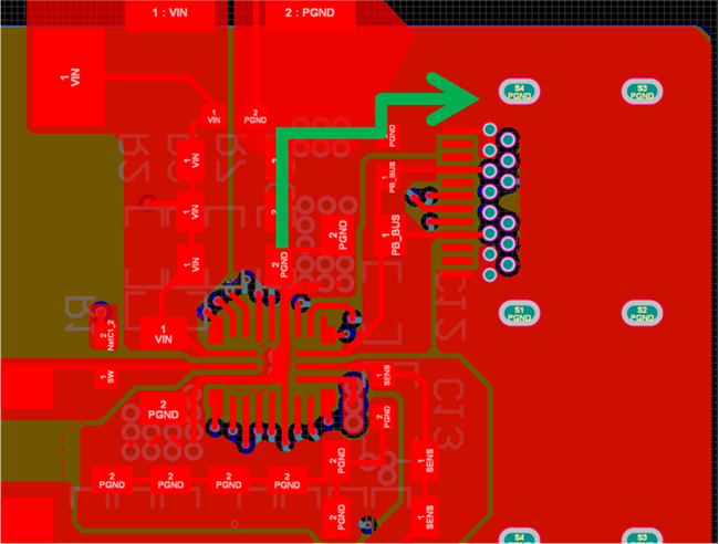
 Figure 5. PGND Layout Example
 As shown in Figure 5, it is an good layout example of ground connection.
With the green path indicated, the ground connection is connected by a big wide copper ground pin and a very short to connector ground pin. The wider trace and shorter trace means smaller parasitic resistor, as well beneficial to heat dissipation. Another benefit of wider and shorter trace have smaller parasitic inductance and capacitor which is better to signal integrity. It is also a good practice to add more vias at PGND to reduce the parasitic resistor and better thermal performance.
For standard or good USB cable, it adopts better conductive medium such as much thicker copper wire and also use advanced shielded wire for signal transmission integrity. Better and thicker conductive medium have smaller wire resistance which mean smaller heat consumption and minor ground shift issue.
LCR meter is sure can being used to measure the cable resistance precisely. Some simple methods can also be adopted to measure the resistance. You can force a small current on the cable and measure the voltage difference of the cable. According to Ohm’s Law, the cable resistance can be easily acquired.
Firstly, you can change control mode from CDP to SDP. As SDP mode allows smaller charging current which means smaller ground shift voltage. If the data communication resumed after mode change, it may be ground shift issue.
Secondly, you can charge the phone to full charging capacity, which means smaller charging current. Then as you attach phone, if the data communication resumed after mode change, it may be ground shift issue.