SLVU192B February 2007 – January 2022 TPS40077
- Trademarks
- 1Introduction
- 2TPS40077EVM-001 Electrical Performance Specifications
- 3Schematic
- 4TPS40077EVM Typical Performance Data and Characteristic Curves
- 5EVM Assembly Drawings and Layout
- 6List of Materials
- 7Revision History
5 EVM Assembly Drawings and Layout
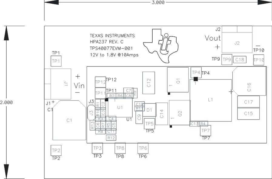
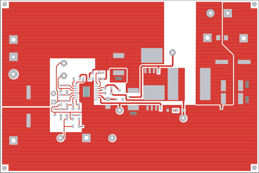
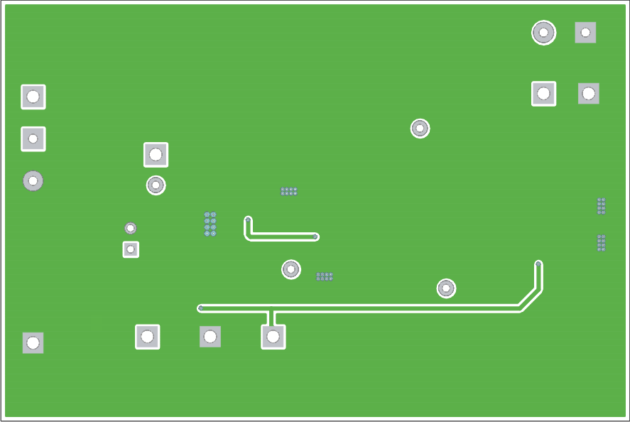
Figure 5-1 through Figure 5-3 show the design of the TPS40077EVM-001 printed circuit board. The EVM has been designed using a double-sided, 2-oz copper-clad circuit board, with all components on the top side to allow the user to easily view, probe, and evaluate the TPS40077 in a practical application. Moving components to both sides of the PCB or using additional internal layers can offer additional size reduction for space-constrained systems.
 Figure 5-1 TPS40077EVM-001 Component Placement (Viewed from Top)
 Figure 5-2 TPS40077EVM-001 Top Copper (Viewed from Top)
 Figure 5-3 TPS40077EVM-001 Bottom Copper (X-Ray View from Top)