SLVU579A December   2011  – September 2021 TPS54427


  1.   Trademarks
  2. 1Introduction
  3. 2Performance Specification Summary
  4. 3Modifications
    1. 3.1 Output Voltage Setpoint
    2. 3.2 Output Filter and Closed-Loop Response
  5. 4Test Setup and Results
    1. 4.1 Input/Output Connections
    2. 4.2 Start-Up Procedure
    3. 4.3 Efficiency
    4. 4.4 Load Regulation
    5. 4.5 Line Regulation
    6. 4.6 Load Transient Response
    7. 4.7 Output Voltage Ripple
    8. 4.8 Input Voltage Ripple
    9. 4.9 Start-Up and Shut-Down
  6. 5Board Layout
    1. 5.1 Layout
  7. 6Schematic, Bill of Materials, and Reference
    1. 6.1 Schematic
    2. 6.2 Bill of Materials
    3. 6.3 Reference
  8. 7Revision History

Load Regulation

The load regulation for the TPS54427 is shown in Figure 4-3. The reference value used to calculate the load regulation is the output voltage value at 2A output current.
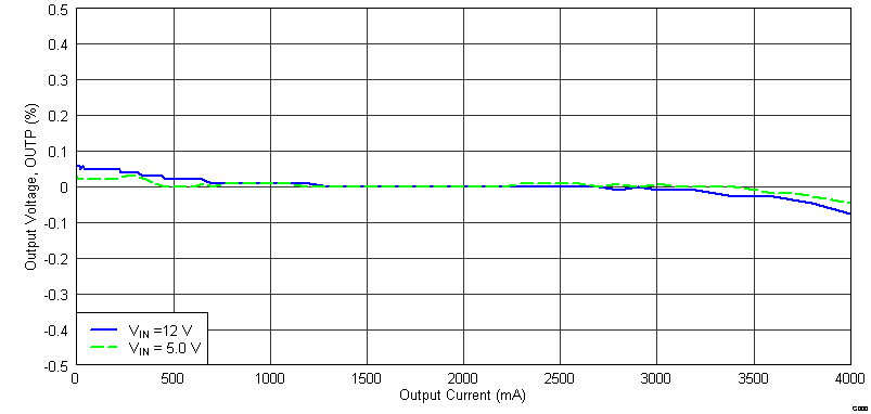
GUID-43361133-7FE6-4665-873C-EE51673032A2-low.pngFigure 4-3 TPS54427 Load Regulation, VIN = 5 V and VIN = 12 V.