SLVUB56A July   2017  – September 2021 TPS54424


  1.   Trademarks
  2. 1Introduction
    1. 1.1 Background
    2. 1.2 Performance Specification Summary
    3. 1.3 Modifications
      1. 1.3.1 Output Voltage Setpoint
      2. 1.3.2 Adjustable UVLO
  3. 2Test Setup and Results
    1. 2.1  Input/Output Connections
    2. 2.2  Efficiency
    3. 2.3  Output Voltage Regulation
    4. 2.4  Load Transient and Loop Response
    5. 2.5  Output Voltage Ripple
    6. 2.6  Input Voltage Ripple
    7. 2.7  Powering Up
    8. 2.8  Powering Down
    9. 2.9  Start-Up Into Pre-Bias
    10. 2.10 Hiccup Mode Current Limit
  4. 3Board Layout
    1. 3.1 Layout
  5. 4Schematic and Bill of Materials
    1. 4.1 Schematic
    2. 4.2 Bill of Materials
  6. 5Revision History

Input Voltage Ripple

Figure 2-10 and Figure 2-11 show the TPS54424EVM-779 input voltage ripple. The load currents are no load and 4 A. VIN = 12 V. The ripple voltage is measured directly across TP1 and TP7.
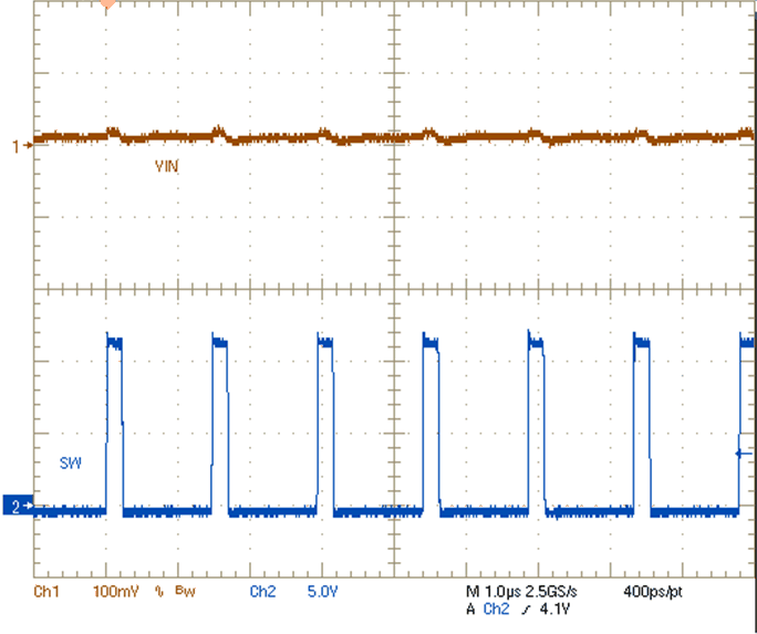
GUID-1B92D1D1-3EBA-4C50-B923-5AAAE0F3AC8E-low.gifFigure 2-10 TPS54424EVM-779 Input Ripple, No Load
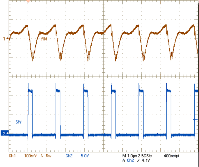
GUID-500CB97C-C0B9-4FCB-A943-F3A94F43BBB8-low.gifFigure 2-11 TPS54424EVM-779 Input Ripple, 4-A Load