SLYT793A may 2020 – may 2020 LM61460-Q1
- 1
- 1 Introduction
- 2 Managing Thermals with Flip-chip Packages
- 3 Board Construction Influence
- 4 Copper Area and Thermals
- 5 Estimating a Converter’s Junction Temperature
- 6 Challenges with Measuring Converter Junction Temperature
- 7 Further Thermal Optimization at the IC Level
- 8 Conclusion
- 9 References
- 10Related Web Sites
7 Further Thermal Optimization at the IC Level
Issues may arise with the thermal performance of the power converter due to cooling limitations. These issues often occur late in the prototype stage. Fortunately, it is possible to change the switching frequency of many converters. A prototype build could allow for the larger or additional component place-holders required for a slower frequency converter.
The switching frequency can heavily impact a converter’s power losses. If a design approaches the maximum recommending operating conditions, a switching frequency adjustment can provide a quick fix to resolve this issue. Reducing the switching frequency will reduce AC losses (switching losses) in the converter, as these losses are directly related to parasitic FET capacitances in the converter and the switching frequency at which they charge and discharge. Additionally, losses in the inductor will drop,[4] although the inductor core material will dictate by how much.
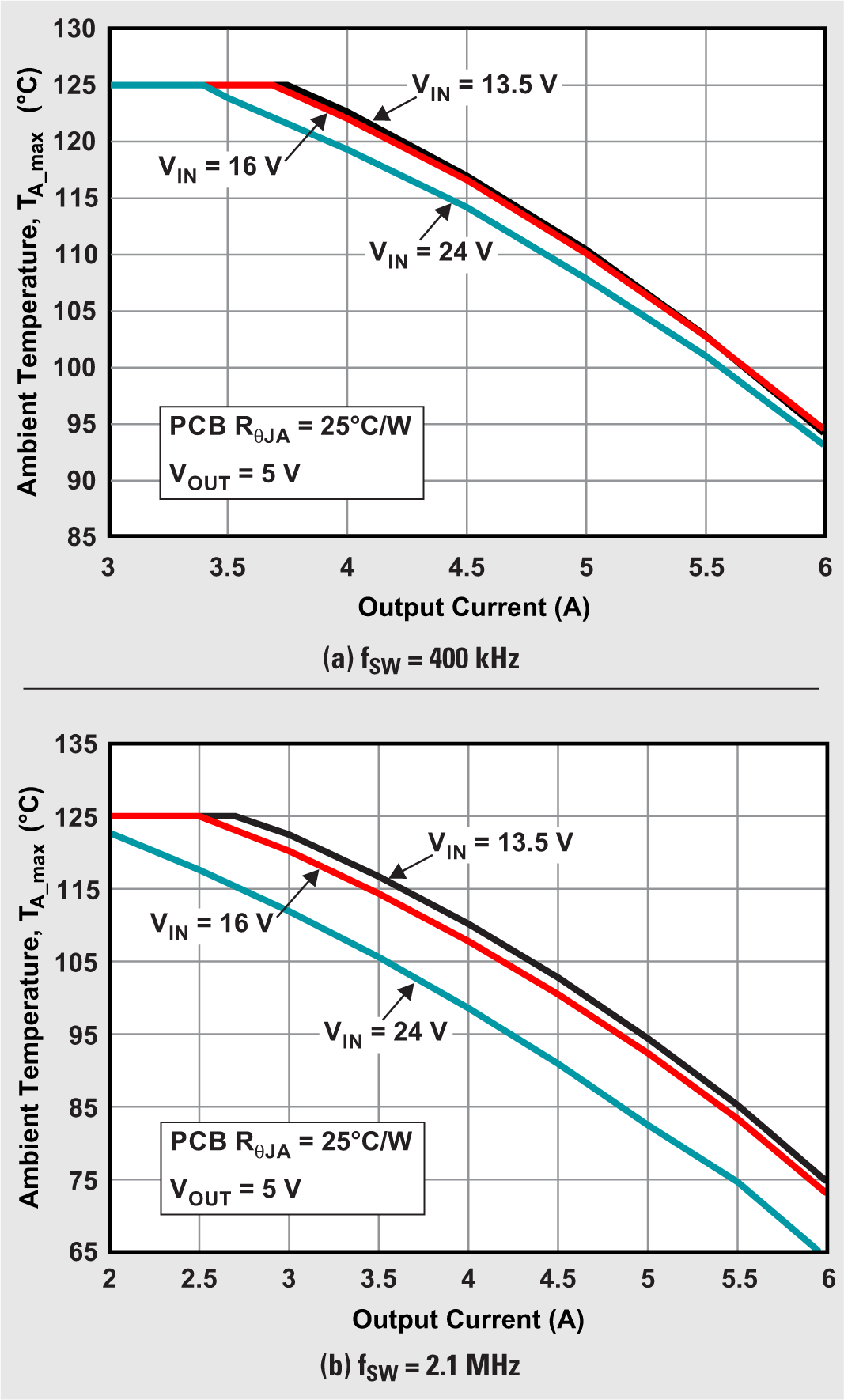
Figure 7 shows the inability of a faster-frequency converter to operate at the same ambient temperature and output power of a slower-frequency converter. Selecting the switching frequency should balance device performance and overall cost for the given application.[5]
One other simple design change to improve thermal performance of the design is proper inductor selection. Changing the inductor to one with lower losses will increase converter design efficiency. The specific losses, AC and DC, are contingent on inductor construction and power conditions. Inductor losses and how they vary with converter specifications can be determined by looking at an inductor’s data sheet.
 Figure 7 Output Power Derating Curves of the LM61460-Q1 Converter
In addition to inductor selection, inductor placement is also a factor in board thermal performance. Sometimes the selected inductor will minimize the solution size and improve the EMI performance of the power supply. Often that inductor will have a very small physical size and a higher DC resistance. This will cause the inductor to heat up, especially at high buck-converter output currents. This can be an issue with designs that have a small switch-node area, as the inductor is crowding the converter and saturating it with heat.
A converter design should balance EMI noise and thermal performance. Having an inductor with a reasonable DC resistance and switch-node area—to allow for heat conduction out of the inductor—will reduce the converter’s RθJA. As EMI standards become more stringent, it is important to carefully consider how large to make the switch-node area because its size will directly impact the radiated noise signature of a buck converter, whose energy will often fall in the most stringent area of the EMI sweep—the FM band.