SLYT793A may 2020 – may 2020 LM61460-Q1
- 1
- 1 Introduction
- 2 Managing Thermals with Flip-chip Packages
- 3 Board Construction Influence
- 4 Copper Area and Thermals
- 5 Estimating a Converter’s Junction Temperature
- 6 Challenges with Measuring Converter Junction Temperature
- 7 Further Thermal Optimization at the IC Level
- 8 Conclusion
- 9 References
- 10Related Web Sites
3 Board Construction Influence
Thermal vias will get heat away from devices mounted on the PCB. Filling vias with conductive material will reduce their thermal resistivity. If via filling is not possible, balancing via copper area and count will allow for effective heat flow.[1]
Making the layer directly underneath the IC as thick and as close to the component layer—by maximizing copper thickness and minimizing dielectric separation—will conduct heat and reduce electromagnetic interference (EMI) most effectively. The total board size must often be a certain height, so the board stackup may need to change.
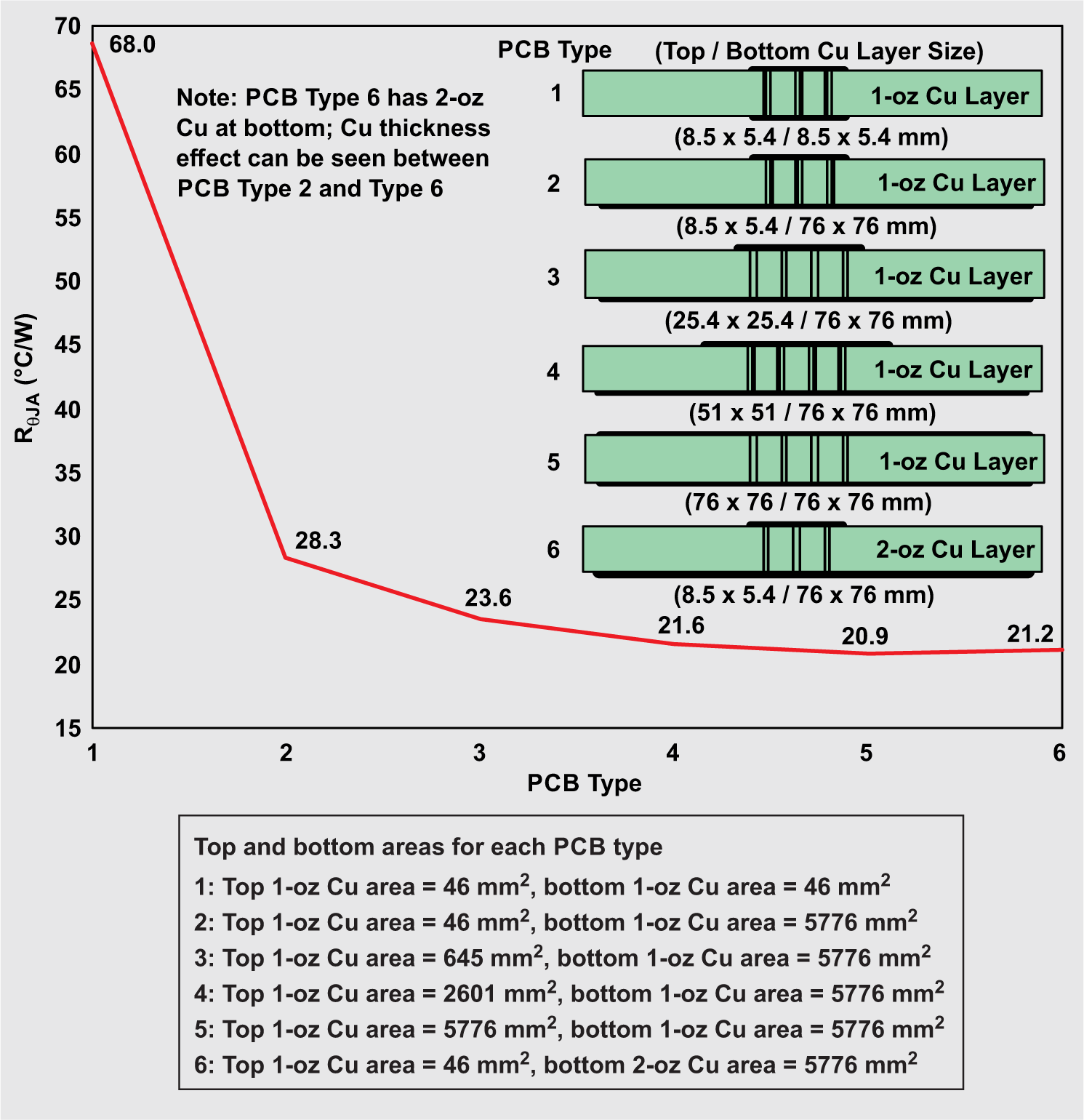
The copper thickness will benefit the board’s thermal performance (Figure 4), which can be quantized by the converter’s effective junction-to-ambient thermal impedance, RθJA.
 Figure 4 Demonstrating the Thermal
Impact between 1- and 2-Oz PCB Copper-layer Weights
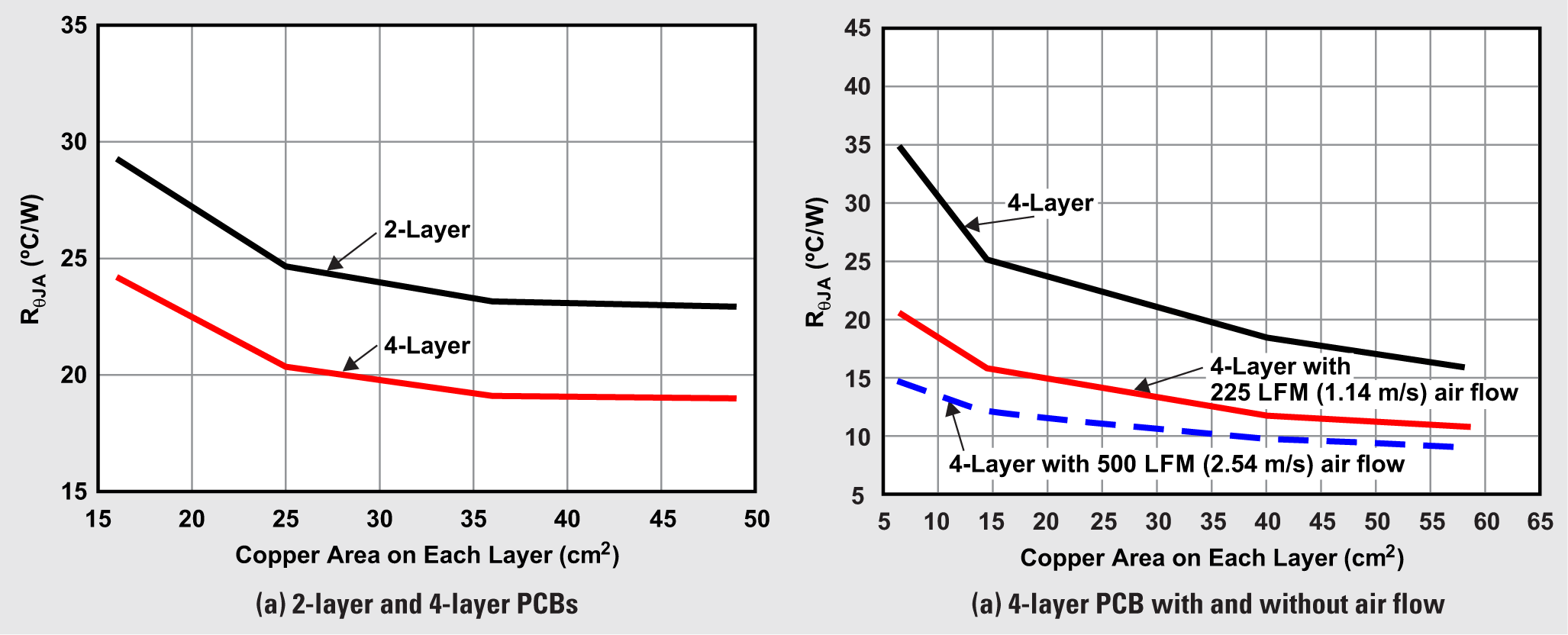
 Figure 5 Effects of Copper Area on
Thermal Performance, RθJA