SNOA961A February   2017  – February 2023 LDC2112 , LDC2114 , LDC3114 , LDC3114-Q1


  1.   Inductive Touch System Design Guide for HMI Button Applications
  2. 1Mechanical Design
    1. 1.1 Theory of Operation
    2. 1.2 Button Construction
    3. 1.3 Mechanical Deflection
    4. 1.4 Mechanical Factors that Affect Sensitivity
      1. 1.4.1 Target Material Selection
        1. 1.4.1.1 Material Stiffness
        2. 1.4.1.2 Material Conductivity
      2. 1.4.2 Button Geometry
      3. 1.4.3 Spacing Between Target and Sensor
    5. 1.5 Layer Stacks of Touch Buttons
      1. 1.5.1 Conductive Surface
      2. 1.5.2 Non-Conductive Surface
    6. 1.6 Sensor Mounting Reference
    7. 1.7 Sensor Mounting Techniques
      1. 1.7.1 Adhesive-Based
      2. 1.7.2 Spring-Based
      3. 1.7.3 Slot-Based
    8. 1.8 Mechanical Isolation
  3. 2Sensor Design
    1. 2.1 Overview
      1. 2.1.1 Sensor Electrical Parameters
      2. 2.1.2 Sensor Frequency
      3. 2.1.3 Sensor RP and RS
      4. 2.1.4 Sensor Inductance
      5. 2.1.5 Sensor Capacitance
      6. 2.1.6 Sensor Quality Factor
    2. 2.2 Inductive Touch
    3. 2.3 LDC211x/LDC3114 Design Boundary Conditions
    4. 2.4 Sensor Physical Construction
      1. 2.4.1 Sensor Physical Size
      2. 2.4.2 Sensor Capacitor Position
      3. 2.4.3 Shielding INn traces
      4. 2.4.4 Shielding Capacitance
      5. 2.4.5 CCOM Sizing
      6. 2.4.6 Multi-Layer Design
        1. 2.4.6.1 Sensor Parasitic Capacitance
      7. 2.4.7 Sensor Spacers
      8. 2.4.8 Sensor Stiffener
      9. 2.4.9 Racetrack Inductor Shape
    5. 2.5 Example Sensor
  4. 3Summary
  5. 4Revision History

Non-Conductive Surface

For non-conductive surfaces such as glass or plastic, a thin sheet of conductive layer, such as aluminum or copper, should be embedded below the surface. When the user presses on the rigid surface at the top of the stack, a micro-deflection is translated onto the conductive layer, bringing the layer closer to the PCB sensor. This alternative approach can extend the application of inductive touch to virtually any material surface.
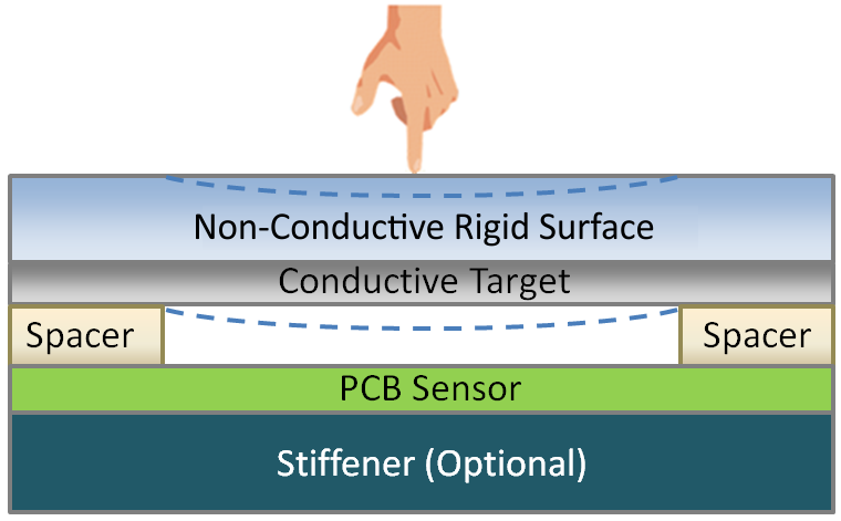
GUID-4F3ADFAC-0A8B-4794-957C-A539C93A036F-low.pngFigure 1-8 Example Layer Stack With Non-Conductive Surface