SNOAA84A January 2022 – February 2022 LM4050QML-SP , LMP7704-SP
Design Steps
- Circuit Specification
- Load power supply (Vbus): 100 V
- Load current (IS1): 1 A to 10 A
- Output voltage (Vout): 0.5 V to 5 V
- Op Amp Selection
The Op-amp common mode voltage (Vcm) needs to be equal to or greater than the bus voltage (Vbus)
- To minimize DC error, an op amp with small offset voltage, offset drift, bias current, and larger CMRR and PSRR are preferred
- Since both input voltages of the op amp are close to Vbus, the maximum common-mode voltage range (CMVR) of the op amp must be equal to or greater than the positive power supply V+ of the op amp
- The LMP7704-SP is selected in this application. This device supports rail to rail input. It has a typical offset voltage of 60 μV, offset drift of 1 μV/°C, bias current of 1 pA, and CMRR of 130 dB. It also has rail-to-rail input and output.
- Shunt Resistor Selection
- Consideration:
- Increasing the shunt resistor value could reduce error but increase power consumption and reduce load supply voltage
- To select a shunt resistor value, the CSM3637 series shunt resistor (data sheet is referenced in the Design References section) is selected to run a simulation in MATLAB®. The tolerance and temperature coefficient of this series of shunt resistors could be down to 0.1% and 10 ppm/°C. Error Calculation shows all equations used for calculating the output error in MATLAB.
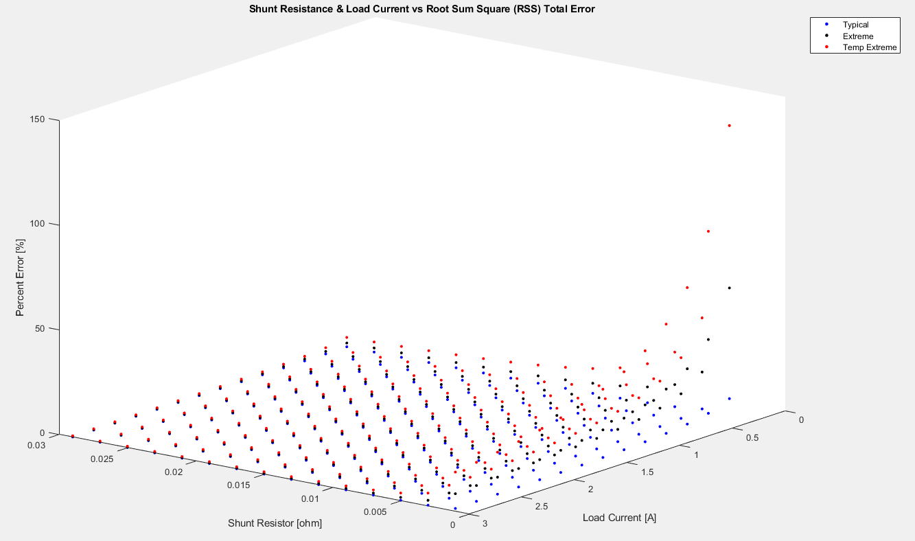
As shown in the previous image, the shunt resistor (Rshunt) and load current (Iload) are used as the inputs for calculating the output percent error. The result shows that the output percent error increases as I_load decreases or R_shunt decreases. Hence, the load current is set to its minimum value (1 A) when picking the R_shunt value to satisfy the minimum requirement in the specification.
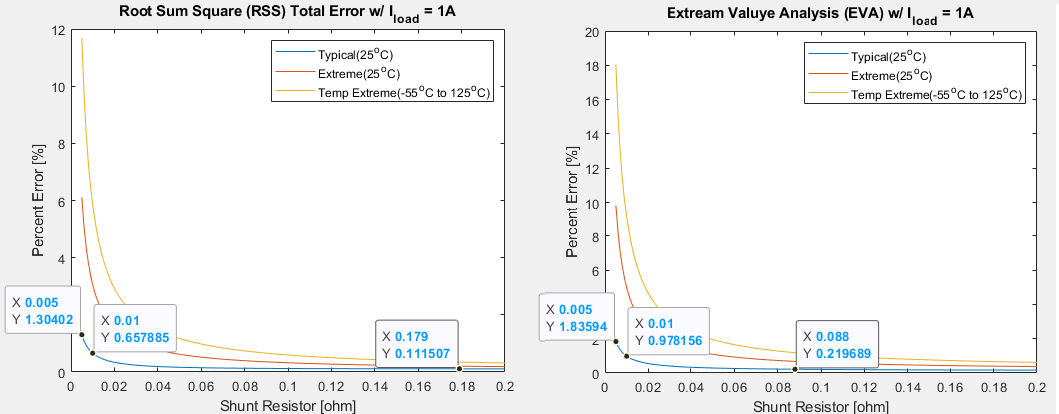
In the following curve, to obtain a root sum square (RSS) error less than 0.7%, a 10-mΩ shunt resistor is selected. Even though increasing R_shunt could further increase accuracy, it also increases power dissipation. The part number of the 10-mΩ CSM series shunt resistor selected is Y14870R00100B9W. The resistor has a power rating up to 3 W. With a derating factor of 0.6 (based on EEE-INST-002), the designed shunt resistor power should be less than 1.8 W. With a maximum load current designed to be 10 A, the maximum power consumed by R_shunt is 1 W, which satisfies the requirement.
- Load voltage supply calculation:
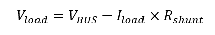
According to the previous equation, with the 10-mΩ (Rshunt) selected, Vload drops from 100 V to 99.9 V.
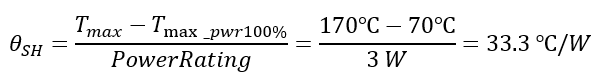
- Shunt resistor self-heating:
With the derating curve found in the shunt resistor data sheet, the self-heating coefficient (θSH) and shunt resistor temperature change (ΔT) are calculated using the following equations.

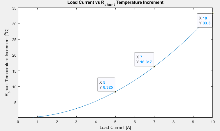
Plugging the previous equations into the MATLAB tool, the relationship between the load current and temperature change is plotted in the following image. From the curve, the shunt resistor temperature is approximately 33.3°C higher than the surrounding temperature with a full load current of 10 A.
- Consideration:
- R5, R6, and R3 Selection
- R6 and R3 calculation
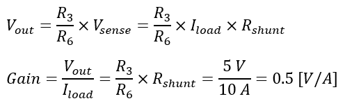
Based on the previous equations, to obtain a Vout range from 0 V to 5 V, with Rshunt equal to 10 mΩ, the ratio of R3 to R6 is calculated to be 50. There are 2 aspects to consider when picking values for R5, R6, and R3:
- To minimize the effect of op amp bias current, R5 is chosen to be the same as R6.
- Increasing R3 and R6 could reduce power consumption but increase minimum Vout due to the effect of Zero Gate Voltage Drain Current (IDSS) of the PMOS.
R6 is set to be 49.9 Ω, and R3 is determined to be 2.49 kΩ for the rest of the calculation. In this application, the Vishay® foil resistor models 303133 to 303138 are selected as a reference for simulation and error calculations. (See the Design References section.)
- R6 and R3 calculation
- PMOS Selection
- The absolute value of the threshold voltage |Vth| of the PMOS needs to be small enough for the op amp to turn the PMOS gate on and off.
- The Zero Gate Voltage Drain Current (IDSS) of the PMOS defines the leakage current when the gate voltage is equal to Vbus. IDSS sets the lower Vout range.
- The PMOS gate capacitance could affect stability if wire resistance from the op amp output (Vo) to the gate is too large. This capacitance adds a zero in the 1/ꞵ curves. If the zero is located on the left of the point where 1/ꞵ and Aol intercept, the phase margin decreases. Hence, a small gate capacitance is preferred.
- Based on military standards, the drain-to-source breakdown voltage must be two times larger than the Vbus, a minimum of 200-V breakdown voltage is required.
PMOS ComparisonParameter IRF9230 IRHE9230 IRHN9250 IRHNJ597230 D-S Breakdown [V] –200 –200 –200 –200 Vgs [V] –2 to –4 –2 to –4 –2 to –4 –2 to –4 Zero Gate Voltage Drain Current [μA] –25 to –250 –25 to –250 –25 to –250 –10 to –25 Input Capacitance [pF] 700 1200 4200 1344 Mounting Type TH SMT SMT SMT Size [mm] 39.37 × 25.53 7.94 × 9.41 16 × 11.55 10.28 × 7.64
As shown in the PMOS Comparison table, IRHNJ597230 is selected because it has the smallest IDSS and has relatively small package size and input capacitance.
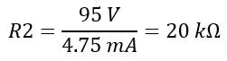
- Shunt Reference and R2 Selection
The shunt reference in the design is to create a virtual voltage supply of 95 V for the LMP7704-SP op amp. The maximum supply current for LMP7704 is 4.5 mA. Hence, the current range of the shunt reference selected must be greater than 4.5 mA.
Shunt Reference Options lists the two shunt reference options for comparison. Both shunt references have a current range greater than 4.5 mA. The reverse breakdown voltage tolerance is not critical in this case, as long as the VEE is around 95 V. Hence, even though the TL1431 has better performance in general, the LM4050QML is preferable because it has a smaller size and requires less components.
Shunt Reference OptionsParameter TL1431-SP LM4050QML-SP Reverse Breakdown Voltage tolerance (%) 0.4 1.75 TID (krad) 100 100 Component Needed 5 3 Current Range (mA) 1 to 100 0.06 to 15 Mounting Type SMT SMT Size (mm) 10.16 × 7.11 6.86 × 10.41 Since the LMP7704 drains a maximum of 4.5 mA, and the shunt reference selected requires at least 0.06 mA, the current through R2 is designed to be 4.75 mA. R2 is calculated with the following formula: