SNOAA84A January 2022 – February 2022 LM4050QML-SP , LMP7704-SP
Design Simulations
- Input and Output Ranges
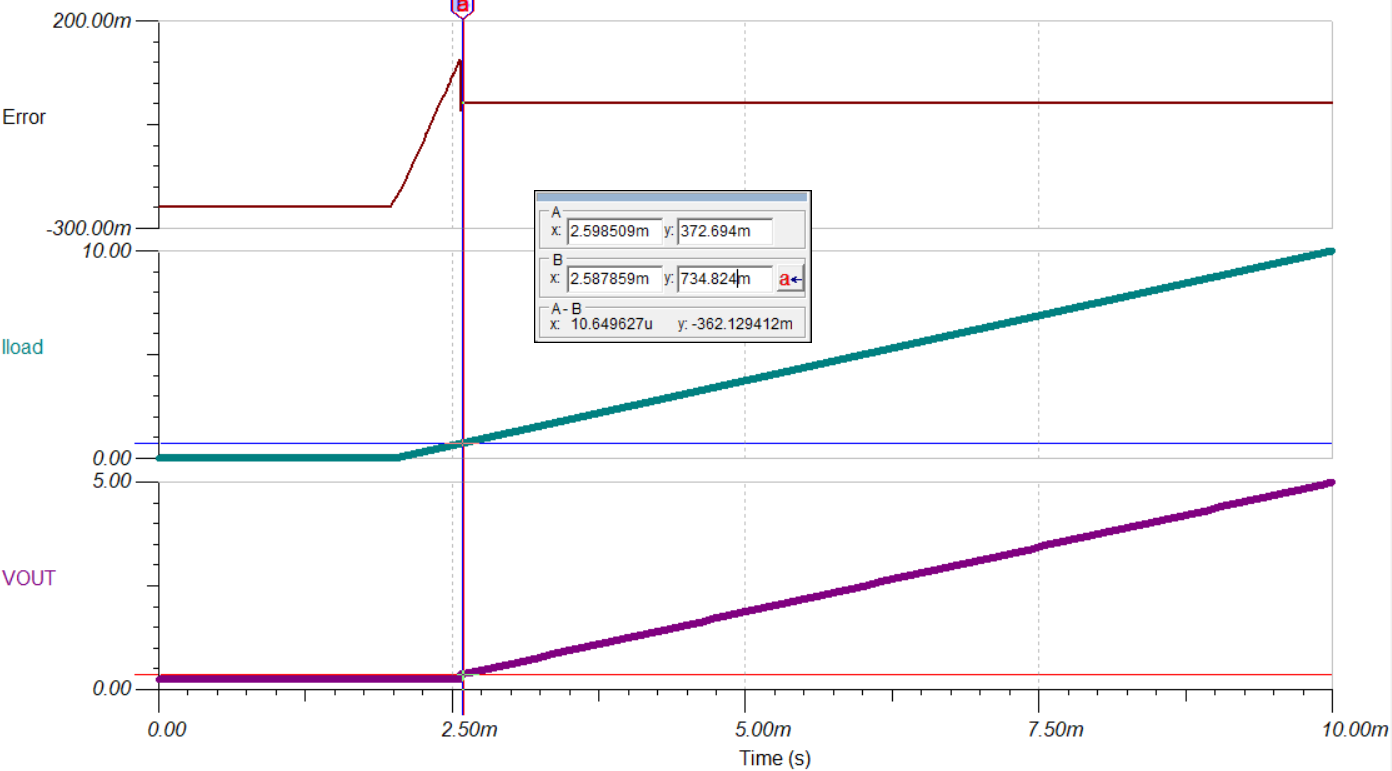
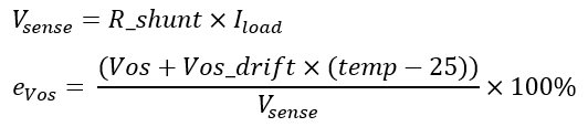
The following plots show the output voltage across the 2.49-kΩ (R3) resistor. The error is calculated based on the following equation:

Ideally, Vout swings from 0 V to 5 V as the load current (Iload) swings from 0 A to 10 A. However, the minimum of Vout is 373 mV and is non-linear before the load current (Iload) gets up to 735 mV.
- Power Consumption
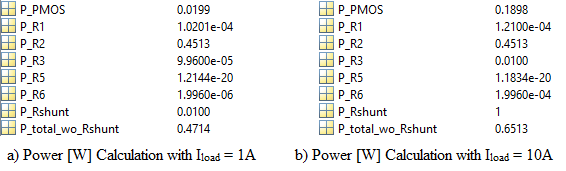
The following simulation and calculations show the power consumption of each component in the circuit with different load currents. Without considering the power consumption on the R_shunt, the overall power rate is from 471.4 mW to 651.3 mW. R2 dominates the power consumption.
- Bandwidth
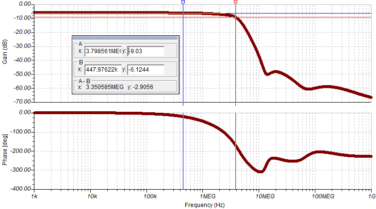
The following figure shows the gain of the circuit, where Gain = Vout (V) / Iload (A). With a load capacitance of 15 pF, the 1% full power bandwidth and the 3-dB bandwidth is found to be 478 kHz and 3.8 MHz.
- Stability Analysis
The stability of the system is verified by measuring its phase margin and applying a small signal-transient step response. To ensure stability, the phase margin, which is measured at a point where the Aol curve intersects 1/β, needs to be at least 45 degrees.
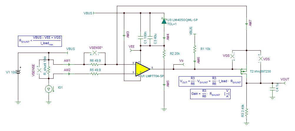
As shown in the following schematic, a 1-μF capacitor is added in the feedback loop to increase stability. The following open-loop AC simulation breaks the loop at the input and the following equations are used to plot the relevant curves:

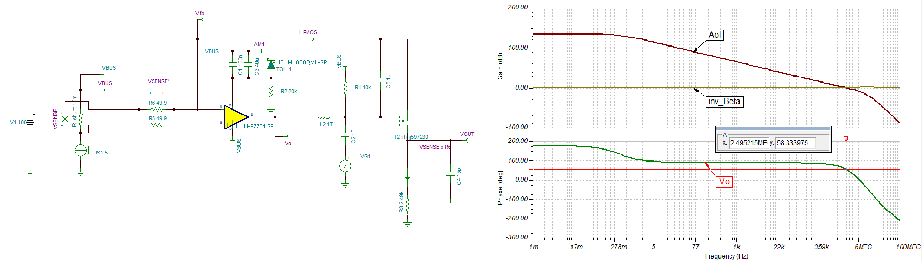
The previous image shows the frequency domain simulation result. The phase margin is measured at a point where 1/ꞵ and Aol intercept, and it is 58.3 degrees, indicating the system is stable.
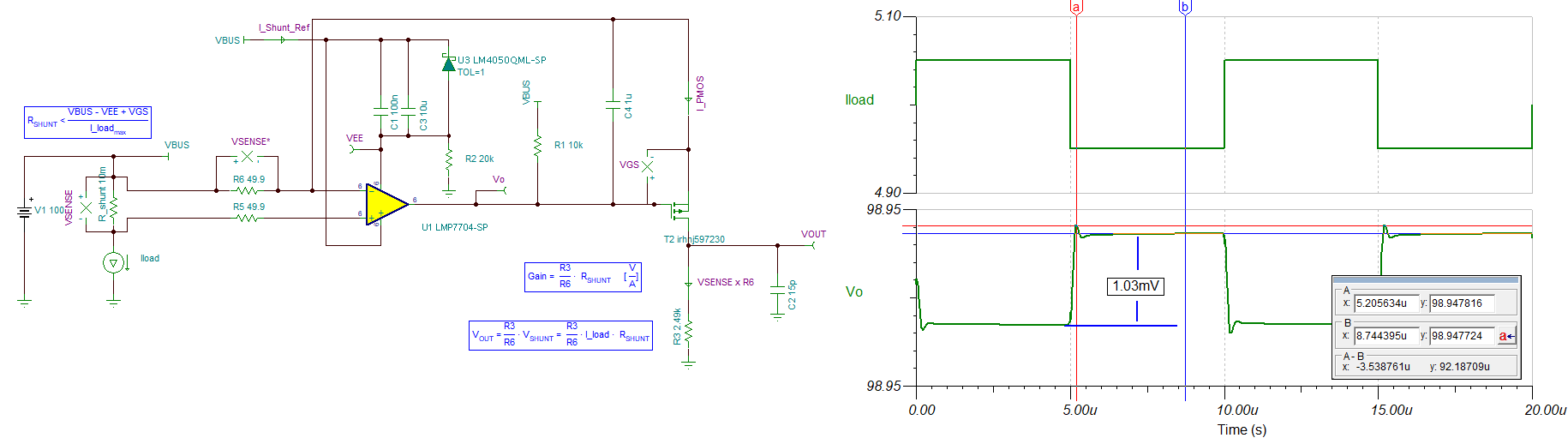
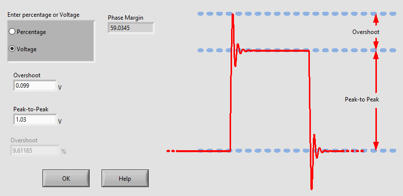
To further ensure stability, a small signal transient step response is applied at the input (IG1) of the circuit and percent overshoot is measured at Vo. The overshoot in the following image indicates a phase margin of 59 degrees, further confirming the stability of the system.
- Fault AnalysisCAUTION: If the LMP7704-SP op amp is damaged and the PMOS gate is left floating, this might destroy the microcontroller or ADC.
It is necessary to put a 10-kΩ pullup resistor (R1) in front of the PMOS gate to pull up the PMOS gate and protect the ADC or microcontroller.
Another fault consideration is whether the op amp (LMP7704-sp) will get damaged by the 100-V Vbus. To simulate it, a 100-V peak-to-peak square wave is applied to the Vbus. See the simulation results in the following image.
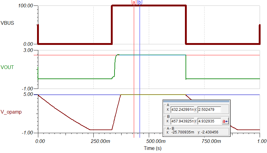
V_opamp, which is the difference between Vbus and VEE, is always below 4.933 V. LMP7704 is designed for a power supply up to 12 V, so it will not be damaged. Load current is set to 5 A in the simulation. As expected, Vout is simulated to be around 2.5 V.
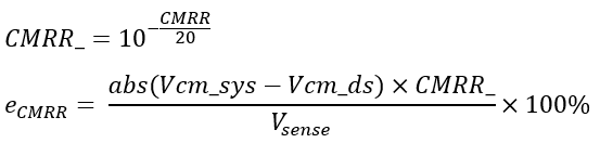
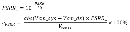
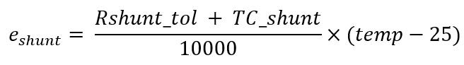
- Error Calculation
To analysis the output error of the circuit, the following parameters are needed
- Vos: Op amp offset error (V)
- Vos_drift: Offset drift (V/°C)
- CMRR: Common-mode rejection ratio (dB)
- PSRR: Power supply rejection ratio (dB)
- temp: temperature (°C)
- Vcm_sys: common-mode voltage (V), 5 V in this application
- Vcm_ds: common-mode voltage used for testing in the data sheet (V).
- R1: R6 resistor value (Ω)
- R_shunt: Shunt resistor value (Ω)
- Rshunt_tol: Shunt resistor tolerance (%)
- TC_shunt: Shunt resistor temperature coefficient (ppm/°C)
- Iload: Load current (A)
- Ib: Input bias current (A)
- R1_tol: R6 resistor tolerance (%)
- TC1: R6 resistor temperature coefficient (ppm/°C)
- R2_tol: R3 resistor tolerance (%)
- TC2: R3 resistor temperature coefficient (ppm/°C)
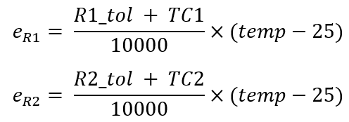
Offset error:
CMRR error:
PSRR error:
Shunt resistor error:
Resistor (R3 and R6) error:
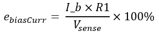
Bias current error:
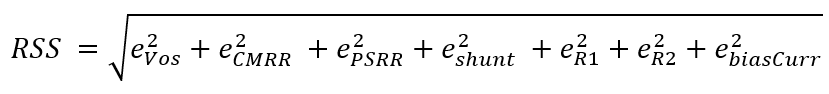
Root Sum Square (RSS) total error:
Extreme Value Analysis (EVA):

The previous error equations are implemented in MATLAB, and the simulation result is shown in the following image.
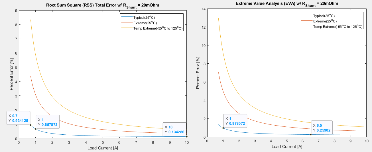
The RSS is 0.658% when the load current is 1 A. This RSS satisfies the 0.7% error requirement. The EVA plot is also provided on the right as a reference.
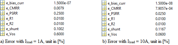
The previous result is calculated with R_shunt set to 10 mΩ. When the load current is 1 A, the op amp Vos dominates the error. When load current is 10 A, the shunt resistor tolerance dominates the error.
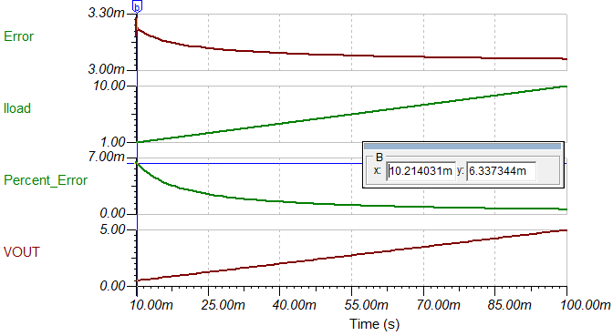
The previous error calculation is verified again with TINA-TITM simulation, and the result is shown in the following image.
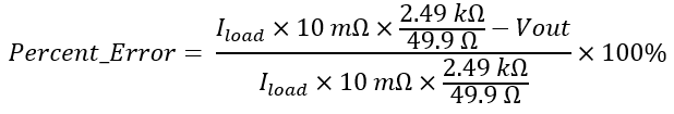
The percent error is calculated with the following equation.
As shown in the simulation, when the load current is 1 A, the error is 0.63%. This error is consistent with the 0.6% Vos error in the previous MATLAB calculation. TINA-TITM does not simulate the error caused by resistor tolerance and changing temperature on the shunt resistor.