SNVA484B October   2011  – March 2024 LM5113


  1.   1
  2.   Description
  3.   IC Features
  4.   4
  5. 1Evaluation Module Overview
    1. 1.1 Introduction
    2. 1.2 Kit Contents
  6. 2Hardware
    1. 2.1 Powering and Loading Considerations
      1. 2.1.1 Proper Board Connection
      2. 2.1.2 Source Power
      3. 2.1.3 Output Current Derating
      4. 2.1.4 Air Flow
      5. 2.1.5 Quick Start-Up Procedure
  7. 3Implementation Results
    1. 3.1 Performance Characteristics
  8. 448V to 3.3V Conversion
  9. 5Hardware Design Files
    1. 5.1 Evaluation Board Schematic
    2. 5.2 PCB Layouts
    3. 5.3 Bill of Materials (BOM)
  10. 6Additional Information
    1. 6.1 Trademarks
  11. 7Revision History

Performance Characteristics

Figure 4-1 shows the efficiency of the LM5113 evaluation board at different input voltage and the load current. 30ns dead time between HI and LI input of the LM5113 is selected to eliminate the shoot through while achieving high efficiency.
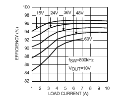
GUID-E5FD45AA-B09E-49A2-950F-5DC82E0A24BD-low.gif Figure 3-1 Evaluation Board Efficiency vs. Load Current

During the dead time, the HS pin voltage can be pulled down below -0.7V and results in an excessive bootstrap voltage. The LM5113 has an internal clamping circuitry that prevents the bootstrap voltage from exceeding 5.25V typically. Figure 4-2 shows the average of the bootstrap voltage with the different load current. As can be seen, the bootstrap voltage is well regulated.
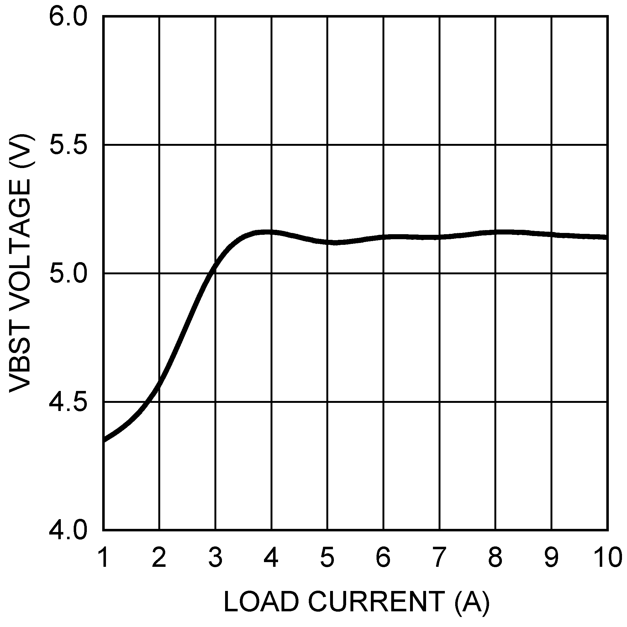
GUID-7B0F4CBF-3144-41F3-A49F-D36232CAED03-low.png Figure 3-2 Bootstrap Voltage Regulation vs. Load Current

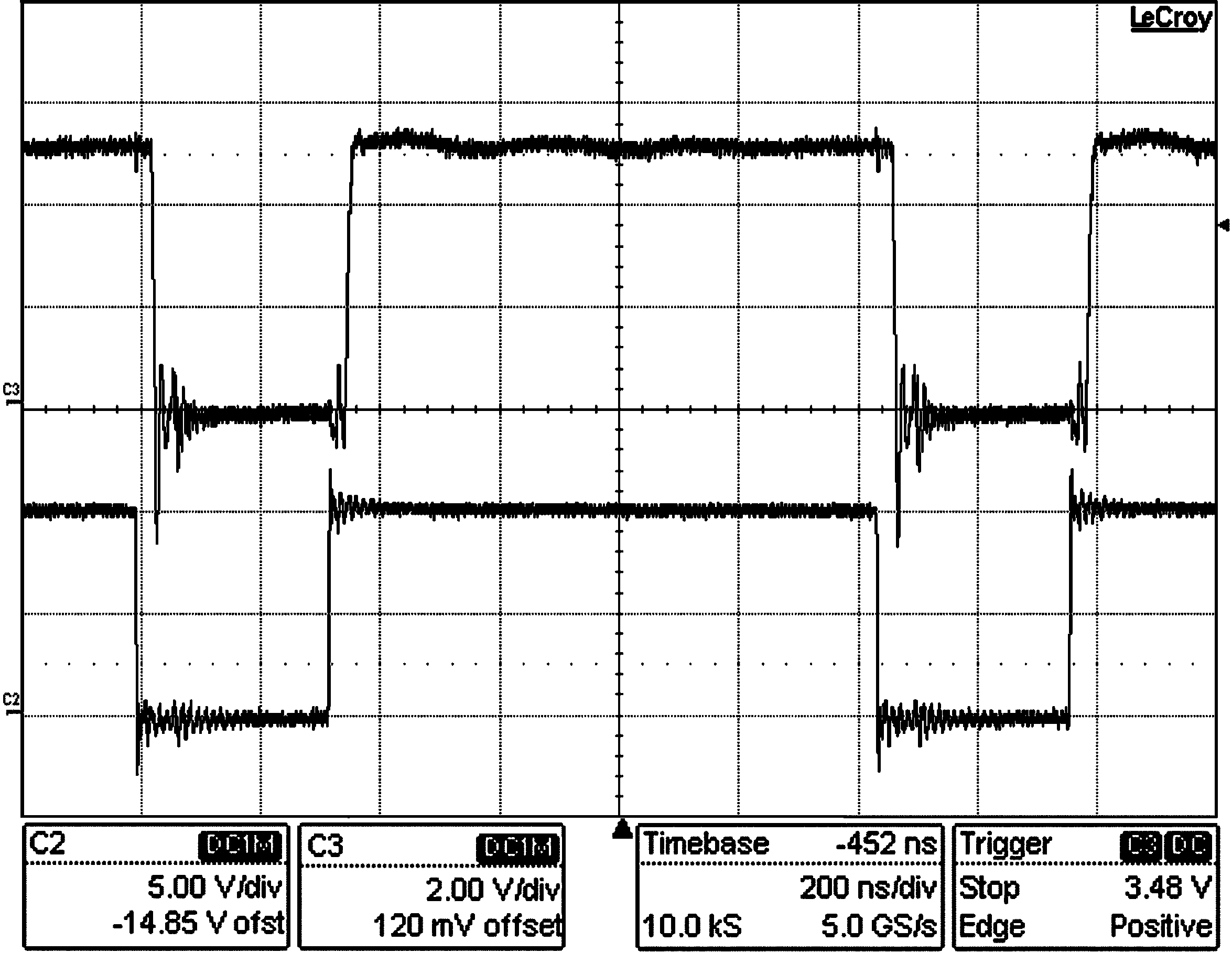
Figure 4-3 compares the input and the output of the low-side driver.
GUID-F7F4F5E4-E9BC-4150-A487-01E29D15F94F-low.png
Conditions: Input Voltage = 48V DC, Load Current = 5A Traces: Top Trace: Gate of Low-Side eGaN FET, Volt/div = 2V Bottom Trace: LI of LM5113, Volt/div = 5V Bandwidth Limit = 600MHz Horizontal Resolution = 0.2µs/div
Figure 3-3 Low-Side Driver Input and Output

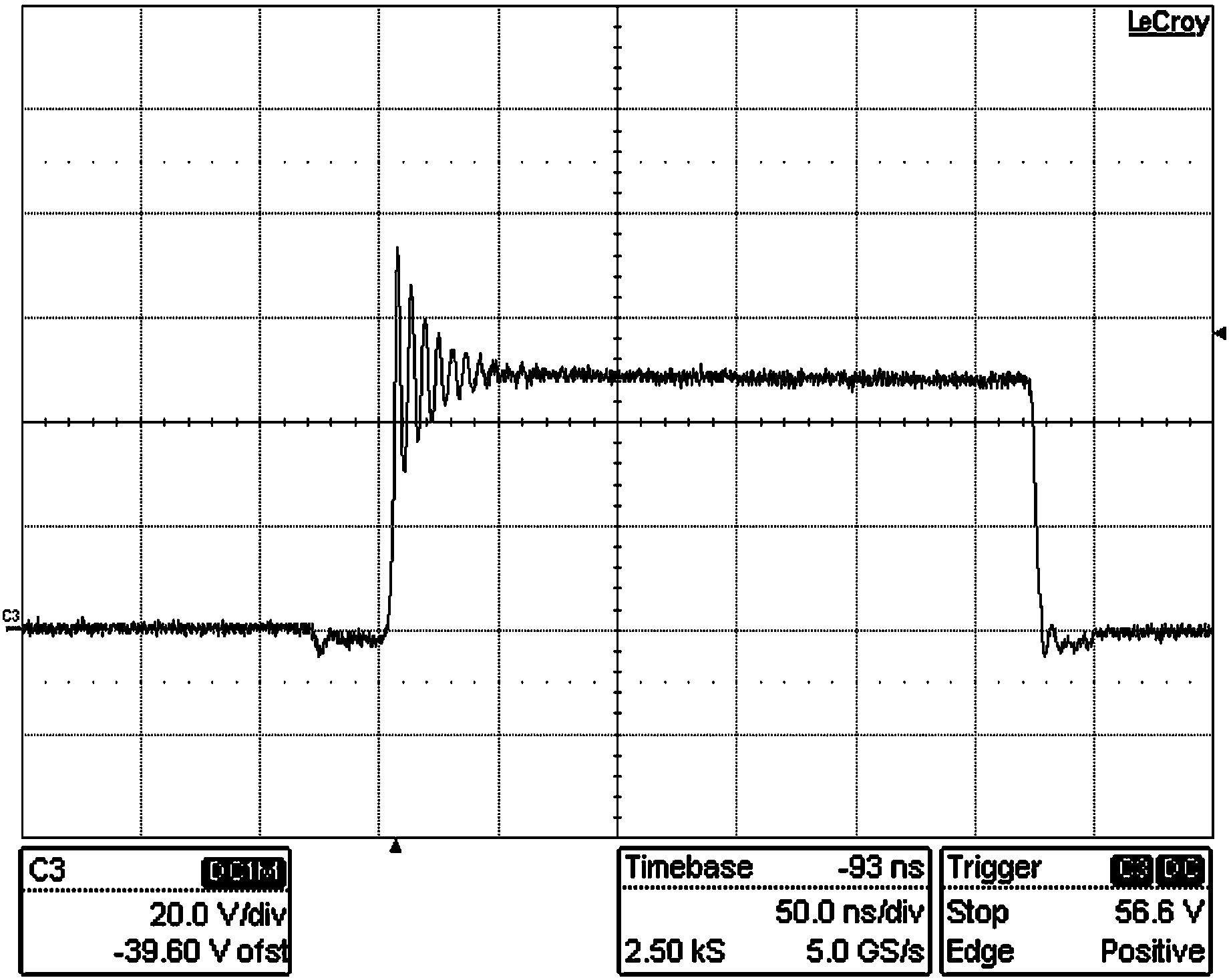
Figure 4-4 shows the switch node voltage that is also the drain voltage of the low-side FET. The ringing on the switch node voltage can be reduced by the HOH gate resistor. 2Ω HOH gate resistance is selected to achieve a drain-source voltage margin of 12V for a 60V input.
GUID-74257AE6-1246-4DD5-9F0C-D00F30A1DCDF-low.png
Conditions: Input Voltage = 48V DC Load Current = 10A Traces: Trace: Switch–Node Voltage, Volts/div = 20V Bandwidth Limit = 600MHz Horizontal Resolution = 50ns/div
Figure 3-4 Switch-Node Voltage

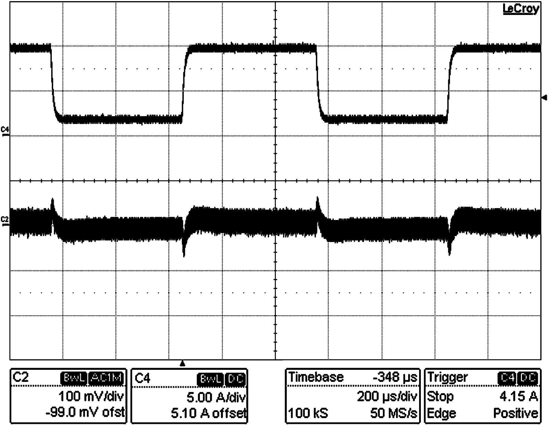
Figure 4-5 shows the load transient response. The load changes between 2A and 10A. 800kHz switching frequency allows the use of a small inductor of 2.7uH, which helps improve the large signal transient response.
GUID-BCAA2F43-5175-402F-94EB-08B1CD440595-low.png
Conditions: Input Voltage = 48V DC Output Current = 2A to 10ATraces: Top Trace: Load Current, Amp/div = 5A Bottom Trace: Output Voltage Volt/div = 100mV, AC coupled Bandwidth Limit = 20MHz Horizontal Resolution = 0.2ms/div
Figure 3-5 Load Transient Response

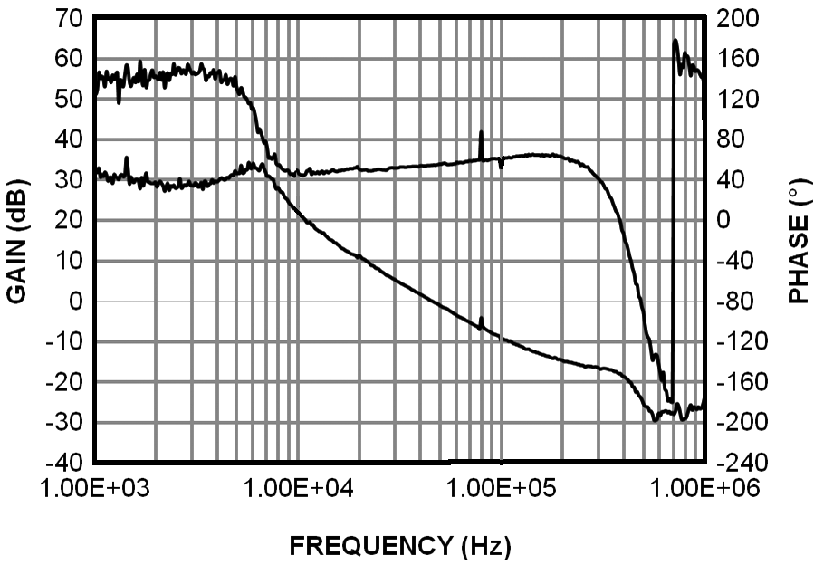
Figure 4-6 shows the measured overall loop response. The crossover frequency is 46kHz and the phase margin is around 55°.
GUID-1AA344BD-8CBC-4A81-A04E-6C06BEC5E15B-low.png
Conditions: Input Voltage = 48V DC Output Current = 10A
Figure 3-6 Loop Gain and Phase