SNVA790A October 2020 – July 2022 LMR36520
2 Fly-Buck Converter Device Operation
The simplest definition of a Fly-Buck™ converter is a synchronous buck converter with the inductor replaced by a coupled inductor and an isolated secondary output. The primary side output is still regulated just like a typical buck converter, and the ideal transfer function from input to primary output is:
The secondary winding of the coupled inductor acts as the source for the secondary output which in its simplest form consists of a rectifier diode and an output capacitor. More components can be added to the secondary output to optimize its performance. See Section 3 for more details. The combination of the rectifying diode and secondary output capacitor provide a DC output voltage to the secondary load determined by Equation 2:
The coupled inductor or transformer provides electrical isolation between primary and secondary outputs, essentially making the secondary float with respect to the primary. Electrical isolation ensures that users are protected from dangerously high voltages which may be present on the input to the device. It is important to note that the secondary output voltage can be either positive or negative with reference to the isolated ground simply by changing the isolated ground location. This is illustrated in Figure 2-2.
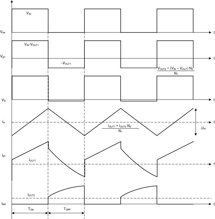
 Figure 2-3 Fly-Buck™ Converter Steady State Waveforms
Figure 2-3 shows the typical steady state waveforms expected of a Fly-Buck™ converter. During the ON-time, the HS or high-side MOSFET is ON and ideally looks like a short circuit. This means that the SW node voltage is equal to the input voltage and the voltage across the primary side of the coupled inductor is VL = VIN - VOUT. Since this is a buck converter, VIN > VOUT so VL is positive during the on-time. The voltage induced across the secondary winding is:
Following the dot convention, the voltage at the dotted terminal of the secondary winding is positive because current enters the dotted terminal of the primary winding. This means that the rectifying diode is therefore reverse biased since the voltage seen at its anode is negative with respect to the isolated ground, and current is supplied to the secondary load by the output capacitor. This reverse bias voltage across the diode during the on-time is given by:
During the off-time, the SW node voltage is pulled down to GND potential due to the LS or low-side MOSFET conducting. The resulting primary winding voltage is:
Following the same procedure as during the ON time, the voltage induced across the secondary winding is now negative at the dotted terminal, which results in the rectifier diode being forward biased. The secondary winding now acts as a current source, as it transfers energy from the primary side to the secondary load. Similar to what happens in normal buck operation, the DC portion of this current is provided to the secondary load while the AC portion of the current charges the secondary output capacitor.