SNVAA89A November 2023 – March 2024 LM75A , LM75B , TMP102 , TMP1075 , TMP110 , TMP112 , TMP112-Q1 , TMP175 , TMP175-Q1 , TMP275 , TMP275-Q1 , TMP75 , TMP75-Q1 , TMP75B , TMP75B-Q1 , TMP75C , TMP75C-Q1
- 1
- Abstract
- Trademarks
- 1 Introduction
- 2 Devices Covered in Application Note: Package Pinout and Spec Compatibility
- 3 Software Compatibility
- 4 TMP1075 Cost-Optimized Dual-Source Layout Using TMP110
- 5 Linux Driver
- 6 Conversion Time and Resolution Setting Highlights
- 7 Interpreting Digital Temperature Output: Data Encoding Compatibility
- 8 Summary
- 9 References
- 10Revision History
4 TMP1075 Cost-Optimized Dual-Source Layout Using TMP110
The TMP110 is a very accurate, cost-effective, and low-power I2C temperature sensor. The dual sourcing feature offers a low-cost advantage, boosts supply chain flexibility, and minimizes risk by allowing more devices in a given circuit design. Dual sourcing incorporates the footprint of two distinct devices within one footprint.
TMP110 is a 5 pin X2Son package, which is a smaller design than the common 8 pin VSSOP and SOIC package typical of the 75 devices. This means that the TMP110 fits within the common 8 pin package. The TMP110 comes in 5 different orderables (Table 4-1). The orderables offer the choice between an alert pin and an address pin. Within the address pin orderables, users can choose between different addresses on the I2C bus. The different orderables are listed in the Table 4-1. The TMP110 has a minimum via drill diameter of 4 mils and a minimum via diameter of 13.78 mils. There are multiple dual source options depending on the number of layers within your PCB.
| GPN | Function | OPN | Device Target Address |
|---|---|---|---|
| TMP110 | Alert | TMP110D0IDPWR | 1001000 |
| TMP110D1IDPWR | 1001001 | ||
| TMP110D2IDPWR | 1001010 | ||
| TMP110D3IDPWR | 1001011 | ||
| Address | TMP110DIDPWR | 1000000 (GND), 1000001 (VDD), 1000010 (SDA), 1000011 (SCL) |
Table 4-2 demonstrates a dual source footprint option between the TMP1075 VSSOP package and the TMP110 which contains an alert pin orderable. Table 4-2 shows the footprint connections between the TMP1075 and the TMP110. The pinouts between the devices are also displayed for reference.
| LM/TMPx75 VSSOP | TMP110 |
|---|---|
| Pin 1 – SDA | Pin 4 – SDA |
| Pin 2 – SCL | Pin 2 – SCL |
| Pin 3 – Alert | Pin 3 – Alert |
| Pin 4 – GND | Pin 1 – GND |
| Pin (5-7) – A0, A1, A2 | Pin 1 – GND |
| Pin 8 – VDD | Pin 5 -VDD |
 Figure 4-1 8-Pin VSSOP Top View
 Figure 4-2 5-Pin X2Son Top View
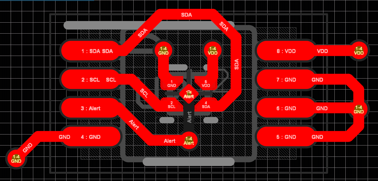
Figure 4-3 and Figure 4-4 show a 3D and a 2D layout trace of the top overview of a 4-layer dual source solution. For simplicity, the displayed boards follow a common four-layer board configuration containing the following layers: Signal, VDD, GND, and Signal. The alert pin on the TMP110 is traced on the bottom layer of the PCB. The vias shown in the 3D and 2D views have a diameter of 16 mil and a hole size of 8 mil. A two layer option is achievable with the aid of the layout trace depicted.
 Figure 4-3 3D Board Image
 Figure 4-4 Top Layer Layout