SPRAAR7J November 2018 – February 2023 66AK2G12 , AM1806 , AM1808 , AM2431 , AM2432 , AM2434 , AM3351 , AM3352 , AM3354 , AM3356 , AM3357 , AM3358 , AM3358-EP , AM3359 , AM3871 , AM3874 , AM3892 , AM3894 , AM4376 , AM4377 , AM4378 , AM4379 , AM5706 , AM5708 , AM5716 , AM5718 , AM5726 , AM5728 , AM5729 , AM5746 , AM5748 , AM5749 , AM620-Q1 , AM623 , AM625 , AM625-Q1 , AM625SIP , AM62A3 , AM62A3-Q1 , AM62A7 , AM62A7-Q1 , AM62P , AM62P-Q1 , AM6411 , AM6412 , AM6421 , AM6422 , AM6441 , AM6442 , AM6526 , AM6528 , AM6546 , AM6548 , BQ24392-Q1 , HD3SS6126 , LP8727 , OMAP-L137 , OMAP5912 , TMS320C6745 , TMS320DM335 , TMS320DM355 , TMS320DM365 , TMS320DM368 , TMS320DM369 , TMS320DM6441 , TMS320DM6443 , TMS320DM6446 , TMS320DM6467 , TMS320DM8127 , TMS320DM8147 , TMS320DM8148 , TMS320DM8165 , TMS320DM8167 , TMS320DM8168 , TMS320VC5506 , TMS320VC5507 , TMS320VC5509A , TS3USB221A-Q1 , TS3USBA225 , TSU5611 , TSU6111 , TSU6111A , TSU6721 , TSU8111
- Abstract
- Trademarks
- 1Introduction
- 2General High-Speed Signal Routing
-
3High-Speed Differential Signal Routing
- 3.1 Differential Signal Spacing
- 3.2 High-Speed Differential Signal Rules
- 3.3 Symmetry in the Differential Pairs
- 3.4 Crosstalk Between the Differential Signal Pairs
- 3.5 Connectors and Receptacles
- 3.6 Via Discontinuity Mitigation
- 3.7 Back-Drill Stubs
- 3.8 Increase Via Anti-Pad Diameter
- 3.9 Equalize Via Count
- 3.10 Surface-Mount Device Pad Discontinuity Mitigation
- 3.11 Signal Bending
- 3.12 Suggested PCB Stackups
- 3.13 ESD/EMI Considerations
- 3.14 ESD/EMI Layout Rules
- 4References
- A Device Layout Parameters
- Revision History
3.10 Surface-Mount Device Pad Discontinuity Mitigation
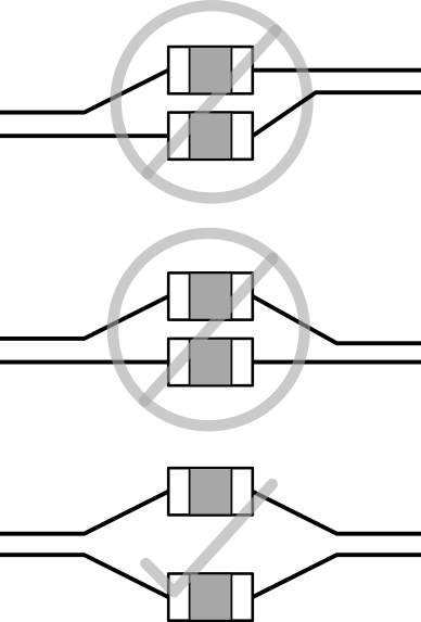
Avoid including surface-mount devices (SMDs) on high-speed signal traces because these devices introduce discontinuities that can negatively affect signal quality. When SMDs are required on the signal traces (for example, the USB SuperSpeed transmit AC coupling capacitors) the maximum permitted component size is 0603. TI strongly recommends using 0402 or smaller. Place these components symmetrically during the layout process to ensure optimum signal quality and to minimize reflection. For examples of correct and incorrect AC coupling capacitor placement, see #SPRAAR7475.
 Figure 3-8 AC-Coupling Placement
To minimize the discontinuities associated with the placement of these components on the differential signal traces, TI recommends voiding the SMD mounting pads of the reference plane by 100%. This void should be at least two PCB layers deep. For an example of a reference plane voiding of surface mount devices, see #SPRAAR77428.
 Figure 3-9 Reference
Plane Voiding of Surface-Mount Devices