SPRACX0 March 2021 TMS320F280021 , TMS320F280021-Q1 , TMS320F280023 , TMS320F280023-Q1 , TMS320F280023C , TMS320F280025 , TMS320F280025-Q1 , TMS320F280025C , TMS320F280025C-Q1 , TMS320F280040-Q1 , TMS320F280040C-Q1 , TMS320F280041 , TMS320F280041-Q1 , TMS320F280041C , TMS320F280041C-Q1 , TMS320F280045 , TMS320F280048-Q1 , TMS320F280048C-Q1 , TMS320F280049 , TMS320F280049-Q1 , TMS320F280049C , TMS320F280049C-Q1 , TMS320F28075 , TMS320F28075-Q1 , TMS320F28076 , TMS320F28374D , TMS320F28374S , TMS320F28375D , TMS320F28375S , TMS320F28375S-Q1 , TMS320F28376D , TMS320F28376S , TMS320F28377D , TMS320F28377D-EP , TMS320F28377D-Q1 , TMS320F28377S , TMS320F28377S-Q1 , TMS320F28378D , TMS320F28378S , TMS320F28379D , TMS320F28379D-Q1 , TMS320F28379S , TMS320F28384D , TMS320F28384D-Q1 , TMS320F28384S , TMS320F28384S-Q1 , TMS320F28386D , TMS320F28386D-Q1 , TMS320F28386S , TMS320F28386S-Q1 , TMS320F28388D , TMS320F28388S , TMS320F28P550SJ , TMS320F28P559SJ-Q1 , TMS320F28P650DH , TMS320F28P650DK , TMS320F28P650SH , TMS320F28P650SK , TMS320F28P659DH-Q1 , TMS320F28P659DK-Q1 , TMS320F28P659SH-Q1
3 PFC CRM/ZVS Realization Based on Type-4 PWM
Figure 3-1 shows the signal interface from external PFC power stage hardware to C2000 internal peripherals to generate PWM signal. This report takes CMPSS5, X-BAR(TRIP5), ePWM1 as an example to explain the realization of CRM/ZVS PFC by type-4 PWM.
 Figure 3-1 Signal Flow Chart
The input signal in Figure 3-1 is the PFC inductor current iL. This is chosen as an input to COMPH positive pin of the CMPSS module as detailed in Figure 3-2. The threshold for capturing current zero crossing (ZC) is a fixed value close to zero and applied to DACHVALS (shadow register DAC value). The current ZC threshold is set as the negative input of COMPH through the reference DAC. The invert output of comparator is chosen as CTRIPH and connected to X-BAR asynchronously.
 Figure 3-2 C2000 MCU CMPSS Block
Diagram
Figure 3-2 C2000 MCU CMPSS Block
DiagramThe CMPSS5 CTRIPH signal connects to X-BAR TRIP5 mux8 as shown in Figure 3-3. In order to pass any signal through to the ePWM, enable the mux8 in the TRIP5MUXENABLE register. CMPSS output is fed into ePWM DC sub-module through ePWM X-BAR. TRIP5, refers to the inductor current negative zero crossing (NZC) event, generates DCAH signals by setting DCAHTRIPSEL.Note that positive zero crossing event is filtered by blanking window as shown in the Figure 3-7. Then, the configuration of TZDCSEL register qualifies the actions on the selected DCAH signal, which generates the DCAEVT1 event. The DCAEVT1 event then is filtered to provide DCAEVT1.sync with a filtered version of the event signals by configuring DCACTL. Then DCAEVT1.sync generates a synchronization pulse to the time-base counter.
 Figure 3-3 X-BAR and ePWM DC Module
Interface
Figure 3-3 X-BAR and ePWM DC Module
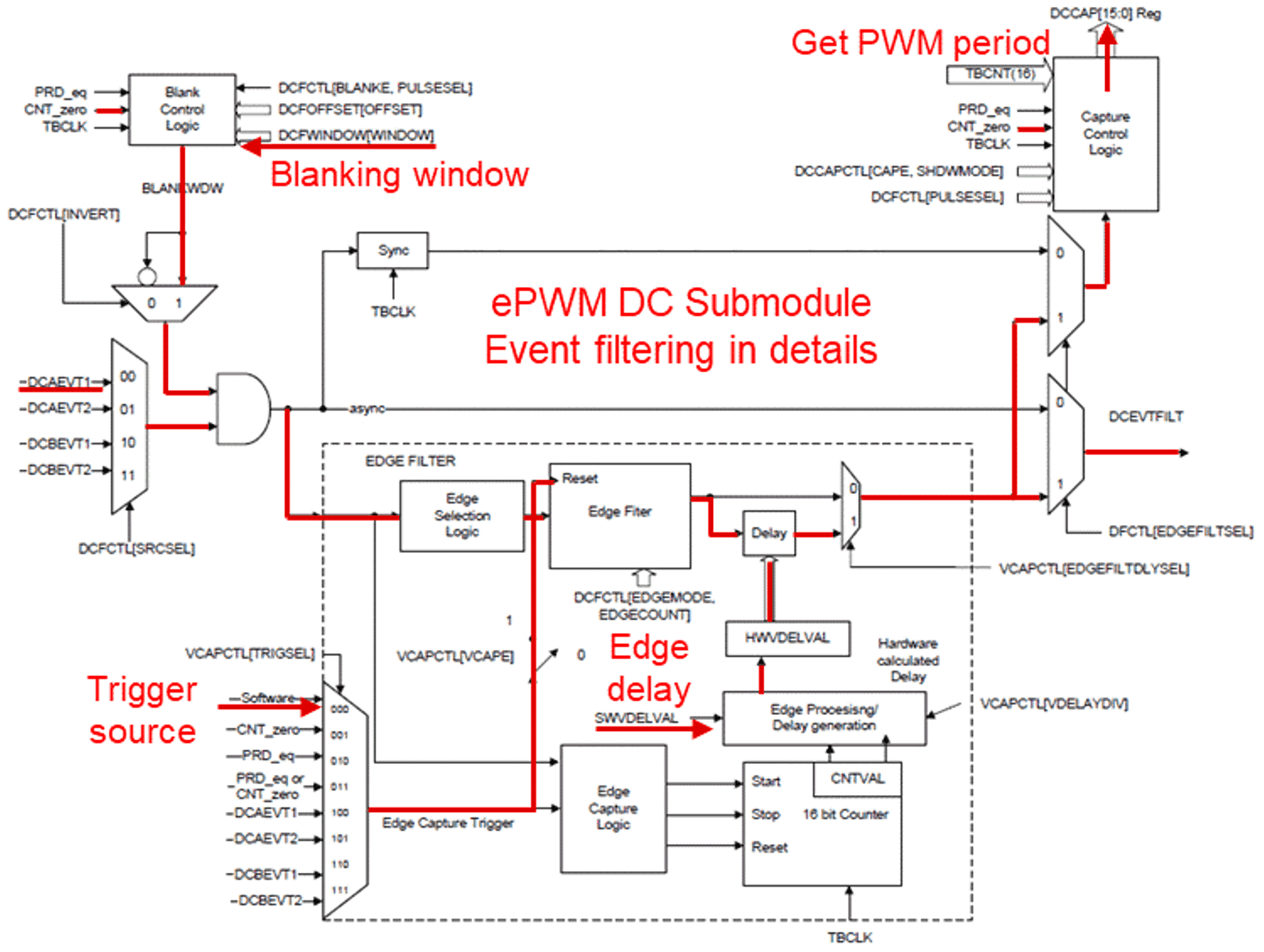
InterfaceDetailed event filtering logic block as shown in Figure 3-4 is critical to realize ZVS/ZCS. The event filtering block can capture the TBCTR value of the trip event to provide control algorithm with PWM period and store the period value in DCCAP register. The blanking logic is used to filter out potential noise and inductor current positive zero crossing (PZC) event on the signal prior to generating right sync signal. Figure 3-4 shows signal flow in the event filtering logic module. Select the DCAEVT1 events as an input to the event filtering logic block (DCFCTL[SRCSEL]) with a blanking window (Blank Control Logic). This is where the comparator output is selected as an input to the event filtering logic block. Blanking window is ANDed with DCAEVT1. Software trigger source is selected as an event to reset and restart the edge filter (VCAPCTL[TRIGSEL]). At the end, configure VCAPCTL[EDGEFILTDLYSEL] to apply delay (a software programmed value in SWVDELVAL) based on the hardware parameters. Now the DCCAP can capture the TBCTR value of the event associated with the inductor current negative zero crossing. This TBCTR value represents the period of the present PWM switching cycle.
 Figure 3-4 Edge Filter and Capture Control
Logic in DC Submodule
Figure 3-4 Edge Filter and Capture Control
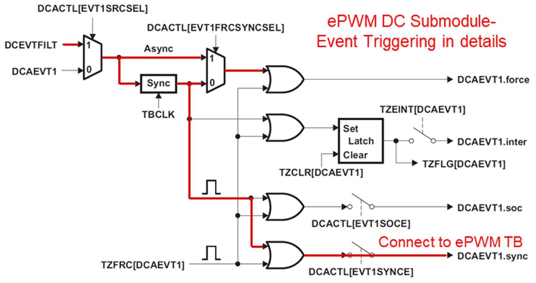
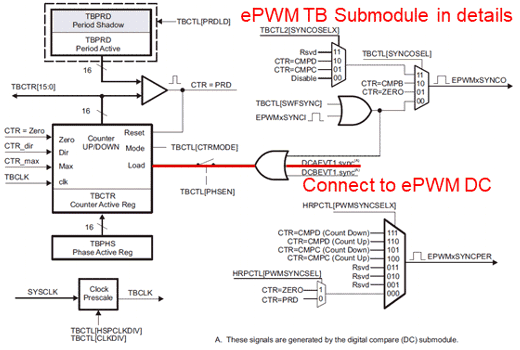
Logic in DC SubmoduleAt the end, DCAEVT1.sync is enabled by set DCACTL[EVT1SYNCE] of event triggering block as shown in Figure 3-5 and phase shift is enabled by setting TBCTL[PHSEN] of time base sub-module to sync TBCTR as shown in Figure 3-6.
 Figure 3-5 Event Triggering Block Used in
CRM/ZVS PFC
 Figure 3-6 Time Base Submodule Used in
CRM/ZVS PFC
Figure 3-6 Time Base Submodule Used in
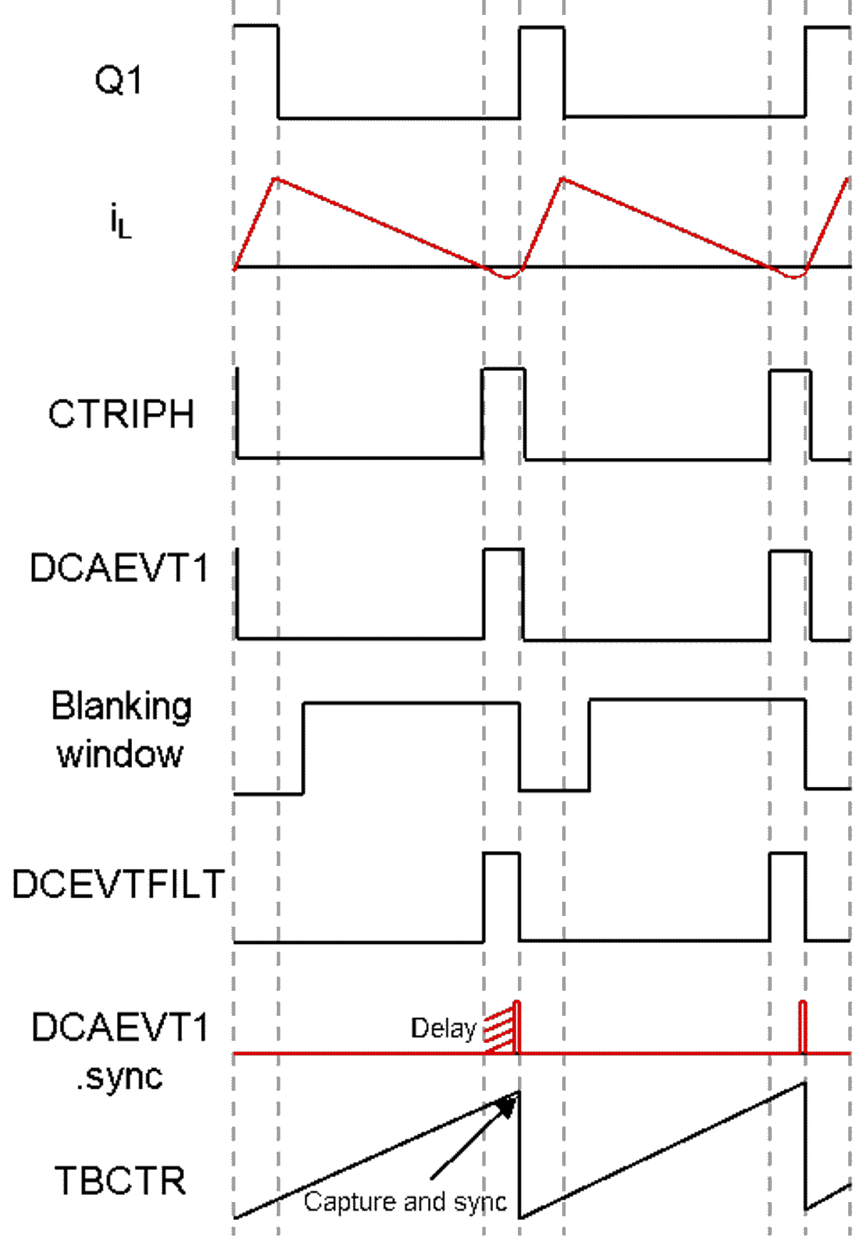
CRM/ZVS PFCFigure 3-7 shows the key signal waveforms after the peripheral configuration. The rising and falling edge of DCAEVT1 signal represents positive and negative zero crossing point accordingly based on Figure 3-7. Blanking window is ANDed with DCAEVT1 to generate DCEVTFILT so that inductor current positive zero crossing (PZC) edge and noise during the MOSFET on-time are filtered. In this way, the blanking window length should be longer than PWM on-time. DC sub-module applies a delay corresponding to inductor negative zero crossing (NZC) edge to generate sync event.
 Figure 3-7 Signal Waveform in CRM PFC Type-4
PWM Implementation