SPRACY9 March 2023 TMS320F2800132 , TMS320F2800132 , TMS320F2800133 , TMS320F2800133 , TMS320F2800135 , TMS320F2800135 , TMS320F2800137 , TMS320F2800137 , TMS320F2800152-Q1 , TMS320F2800152-Q1 , TMS320F2800153-Q1 , TMS320F2800153-Q1 , TMS320F2800154-Q1 , TMS320F2800154-Q1 , TMS320F2800155 , TMS320F2800155 , TMS320F2800155-Q1 , TMS320F2800155-Q1 , TMS320F2800156-Q1 , TMS320F2800156-Q1 , TMS320F2800157 , TMS320F2800157 , TMS320F2800157-Q1 , TMS320F2800157-Q1 , TMS320F280021 , TMS320F280021 , TMS320F280021-Q1 , TMS320F280021-Q1 , TMS320F280023 , TMS320F280023 , TMS320F280023-Q1 , TMS320F280023-Q1 , TMS320F280023C , TMS320F280023C , TMS320F280025 , TMS320F280025 , TMS320F280025-Q1 , TMS320F280025-Q1 , TMS320F280025C , TMS320F280025C , TMS320F280025C-Q1 , TMS320F280025C-Q1 , TMS320F280033 , TMS320F280033 , TMS320F280034 , TMS320F280034 , TMS320F280034-Q1 , TMS320F280034-Q1 , TMS320F280036-Q1 , TMS320F280036-Q1 , TMS320F280036C-Q1 , TMS320F280036C-Q1 , TMS320F280037 , TMS320F280037 , TMS320F280037-Q1 , TMS320F280037-Q1 , TMS320F280037C , TMS320F280037C , TMS320F280037C-Q1 , TMS320F280037C-Q1 , TMS320F280038-Q1 , TMS320F280038-Q1 , TMS320F280038C-Q1 , TMS320F280038C-Q1 , TMS320F280039 , TMS320F280039 , TMS320F280039-Q1 , TMS320F280039-Q1 , TMS320F280039C , TMS320F280039C , TMS320F280039C-Q1 , TMS320F280039C-Q1 , TMS320F280040-Q1 , TMS320F280040-Q1 , TMS320F280040C-Q1 , TMS320F280040C-Q1 , TMS320F280041 , TMS320F280041 , TMS320F280041-Q1 , TMS320F280041-Q1 , TMS320F280041C , TMS320F280041C , TMS320F280041C-Q1 , TMS320F280041C-Q1 , TMS320F280045 , TMS320F280045 , TMS320F280048-Q1 , TMS320F280048-Q1 , TMS320F280048C-Q1 , TMS320F280048C-Q1 , TMS320F280049 , TMS320F280049 , TMS320F280049-Q1 , TMS320F280049-Q1 , TMS320F280049C , TMS320F280049C , TMS320F280049C-Q1 , TMS320F280049C-Q1 , TMS320F28075 , TMS320F28075 , TMS320F28075-Q1 , TMS320F28075-Q1 , TMS320F28076 , TMS320F28076 , TMS320F28374D , TMS320F28374D , TMS320F28374S , TMS320F28374S , TMS320F28375D , TMS320F28375D , TMS320F28375S , TMS320F28375S , TMS320F28375S-Q1 , TMS320F28375S-Q1 , TMS320F28376D , TMS320F28376D , TMS320F28376S , TMS320F28376S , TMS320F28377D , TMS320F28377D , TMS320F28377D-EP , TMS320F28377D-EP , TMS320F28377D-Q1 , TMS320F28377D-Q1 , TMS320F28377S , TMS320F28377S , TMS320F28377S-Q1 , TMS320F28377S-Q1 , TMS320F28378D , TMS320F28378D , TMS320F28378S , TMS320F28378S , TMS320F28379D , TMS320F28379D , TMS320F28379D-Q1 , TMS320F28379D-Q1 , TMS320F28379S , TMS320F28379S , TMS320F28384D , TMS320F28384D , TMS320F28384D-Q1 , TMS320F28384D-Q1 , TMS320F28384S , TMS320F28384S , TMS320F28384S-Q1 , TMS320F28384S-Q1 , TMS320F28386D , TMS320F28386D , TMS320F28386D-Q1 , TMS320F28386D-Q1 , TMS320F28386S , TMS320F28386S , TMS320F28386S-Q1 , TMS320F28386S-Q1 , TMS320F28388D , TMS320F28388D , TMS320F28388S , TMS320F28388S , TMS320F28P650DH , TMS320F28P650DH , TMS320F28P650DK , TMS320F28P650DK , TMS320F28P650SH , TMS320F28P650SH , TMS320F28P650SK , TMS320F28P650SK , TMS320F28P659DH-Q1 , TMS320F28P659DH-Q1 , TMS320F28P659DK-Q1 , TMS320F28P659DK-Q1 , TMS320F28P659SH-Q1 , TMS320F28P659SH-Q1
- Abstract
- Trademarks
- 1Introduction
- 2Input Settling Design Steps
-
3Example Circuit Design
- 3.1 Select the ADC
- 3.2 Find the Minimum Op-Amp Bandwidth and RC Filter Ranges
- 3.3 Verify the Op-Amp Model
- 3.4 Build the ADC Input Model
- 3.5 Bias Point Analysis to Determine Voa_ss
- 3.6 Transient Analysis to Determine Voa_ss
- 3.7 Perform Initial Transient Analysis
- 3.8 Iterative Approach to Refine RC Filter Values
- 3.9 Perform Final Transient Analysis
- 3.10 Perform Final Transient Analysis
- 3.11 Further Refinement
- 3.12 Further Simulations
- 3.13 Completed Worksheet
- 4Working With Existing Circuits or Additional Constraints
- 5Summary
- 6References
4.1.2 Charge Sharing Example
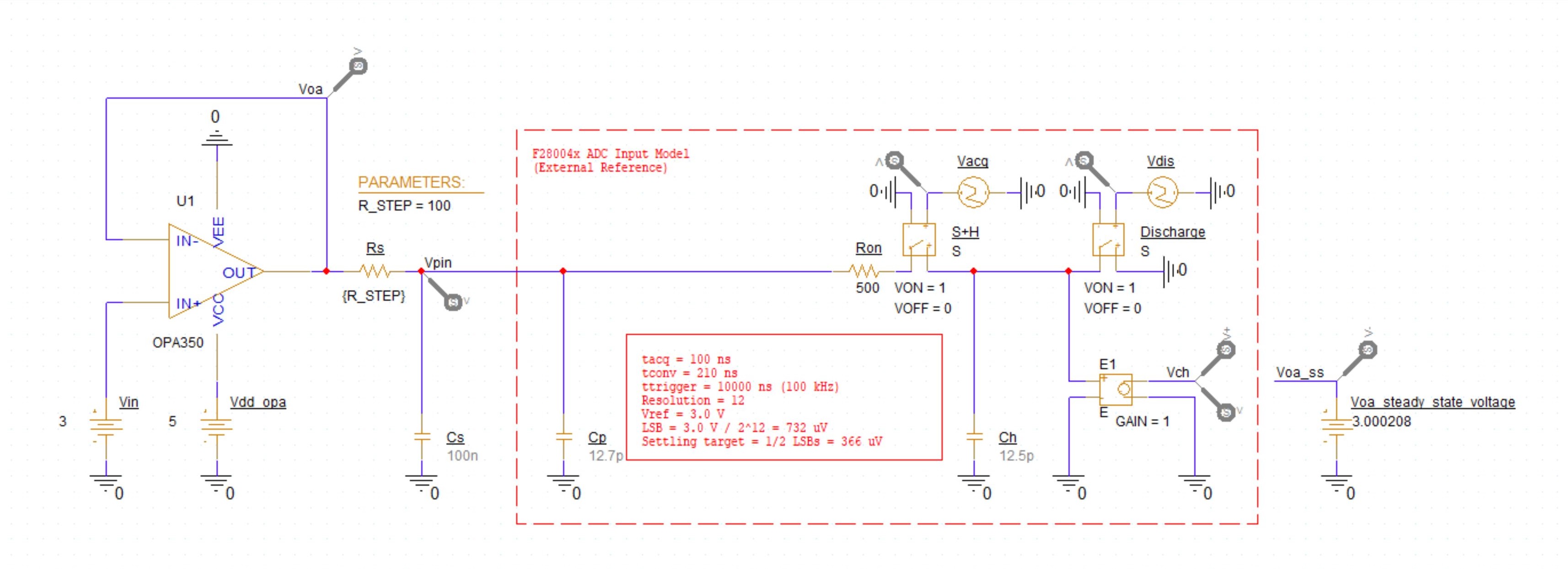
In the example circuit in Figure 4-1, Cs has been set to approximately 2(N+1) x Ch and the sample trigger rate is set to 100 kHz.
 Figure 4-1 Example Circuit Utilizing
Charge Sharing
Figure 4-1 Example Circuit Utilizing
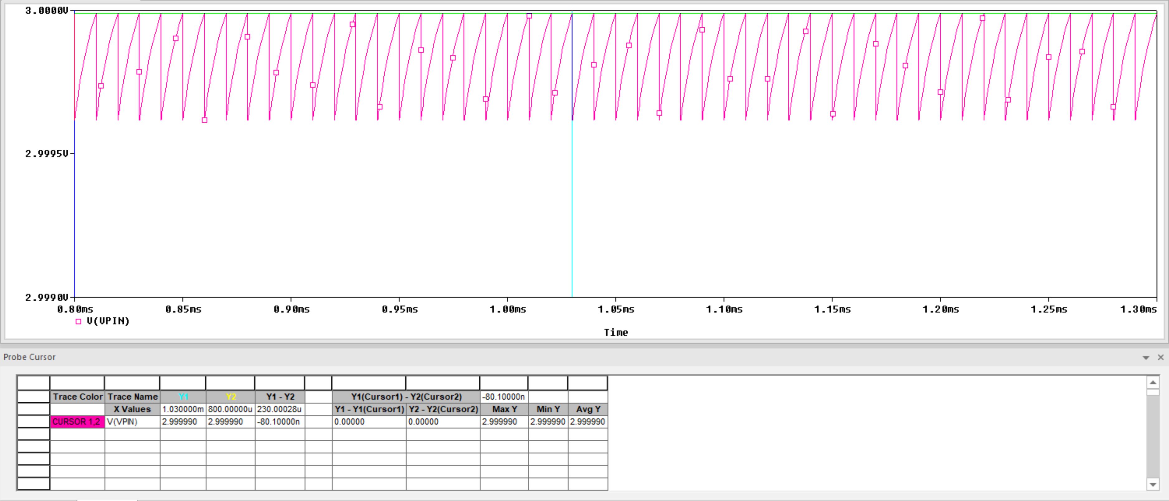
Charge SharingFigure 4-2 shows the pin transient over many sampling cycles when Rs is 100 Ω. It can be seen that the voltage on the pin (which is the voltage directly on Cs) recovers to within 1/2 LSBs in the time between conversions. This will result in good ADC input settling using a very short S+H window as long as the sample-rate remains at or below 100 ksps.
 Figure 4-2 Cs Voltage With
Rs = 100 Ω
Figure 4-2 Cs Voltage With
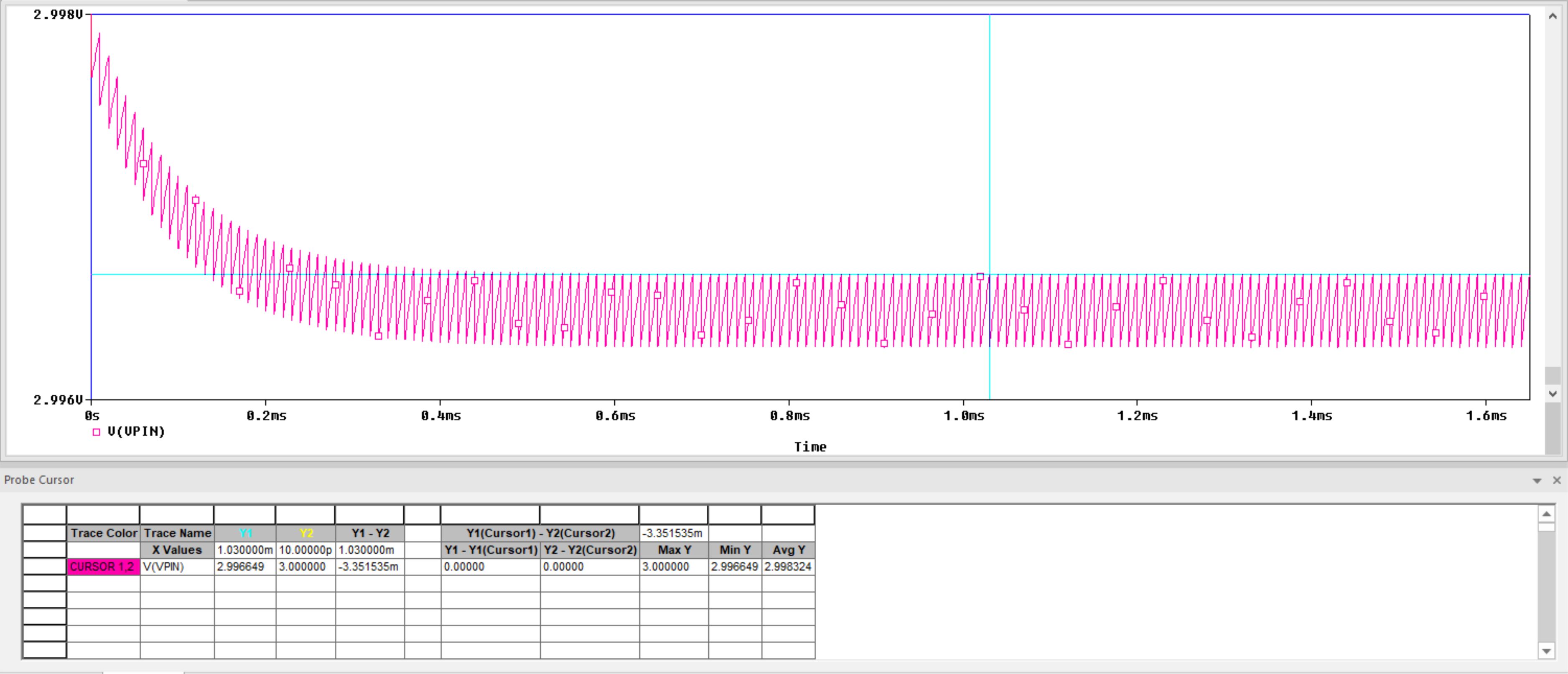
Rs = 100 ΩNow consider the results in Figure 4-3. Rs has been set to 1k Ω. In this case, the voltage on Cs is slowly depleted sample-by-sample until an equilibrium is reached. At equilibrium, the pin voltage has an error of about 3.5 mV. Even though Ch will quickly match the Cs voltage during the S+H phase, the voltage on Cs has a significant error.
 Figure 4-3 Cs Voltage With
Rs = 1k Ω
Figure 4-3 Cs Voltage With
Rs = 1k ΩTo resolve this error, either Rs would need to be decreased or the sample rate would have to be reduced.
This example underscores the importance of simulating circuits with large Cs or Rs over many cycles.