SPRAD15 March 2022 TMS320F280021 , TMS320F280021-Q1 , TMS320F280023 , TMS320F280023-Q1 , TMS320F280023C , TMS320F280025 , TMS320F280025-Q1 , TMS320F280025C , TMS320F280025C-Q1 , TMS320F280033 , TMS320F280034 , TMS320F280034-Q1 , TMS320F280036-Q1 , TMS320F280036C-Q1 , TMS320F280037 , TMS320F280037-Q1 , TMS320F280037C , TMS320F280037C-Q1 , TMS320F280038-Q1 , TMS320F280038C-Q1 , TMS320F280039 , TMS320F280039-Q1 , TMS320F280039C , TMS320F280039C-Q1 , TMS320F280040-Q1 , TMS320F280040C-Q1 , TMS320F280041 , TMS320F280041-Q1 , TMS320F280041C , TMS320F280041C-Q1 , TMS320F280045 , TMS320F280048-Q1 , TMS320F280048C-Q1 , TMS320F280049 , TMS320F280049-Q1 , TMS320F280049C , TMS320F280049C-Q1 , TMS320F28075 , TMS320F28075-Q1 , TMS320F28076 , TMS320F28374D , TMS320F28375D , TMS320F28376D , TMS320F28377D , TMS320F28377D-EP , TMS320F28377D-Q1 , TMS320F28378D , TMS320F28379D , TMS320F28379D-Q1 , TMS320F28384D , TMS320F28384D-Q1 , TMS320F28384S , TMS320F28384S-Q1 , TMS320F28386D , TMS320F28386D-Q1 , TMS320F28386S , TMS320F28386S-Q1 , TMS320F28388D , TMS320F28388S , TMS320F28P550SJ , TMS320F28P559SJ-Q1 , TMS320F28P650DH , TMS320F28P650DK , TMS320F28P650SH , TMS320F28P650SK , TMS320F28P659DH-Q1 , TMS320F28P659DK-Q1 , TMS320F28P659SH-Q1
2.1 Primary Side
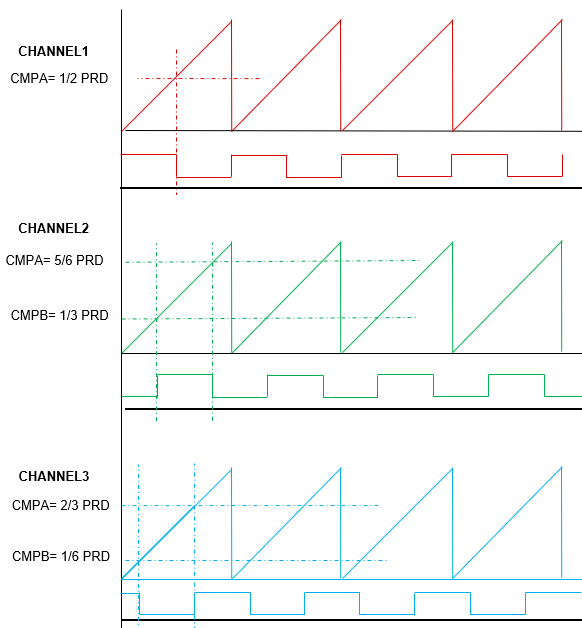
Firstly, Figure 2-1 demonstrates how the primary side PWM control signal of a 3-phase interleaved LLC could be generated. Assuming PWM 1/2/3 represents he PWM signal of phase A/B/C, respectively, 120° phase shift is required between each phase to achieve 3-phase interleaved LLC. To achieve this, CMPA is set to 1/3*PRD, while CMPB is set to 5/6*PRD for channel 2, and CMPA is set to 2/3*PRD, while CMPB is set to 1/6*PRD for channel 3. By configuring channel 2 and channel 3's toggling action as shown in Figure 2-1, a 120° phase shift can be achieved.
 Figure 2-1 Primary Side PWM
Waveform
Figure 2-1 Primary Side PWM
WaveformSpecial consideration is needed when the frequency changes. Since CMPA/CMPB values are calculated from PWM, they must be loaded simultaneously to avoid the mismatch of PWM period and phase shifting between three PWM phases.
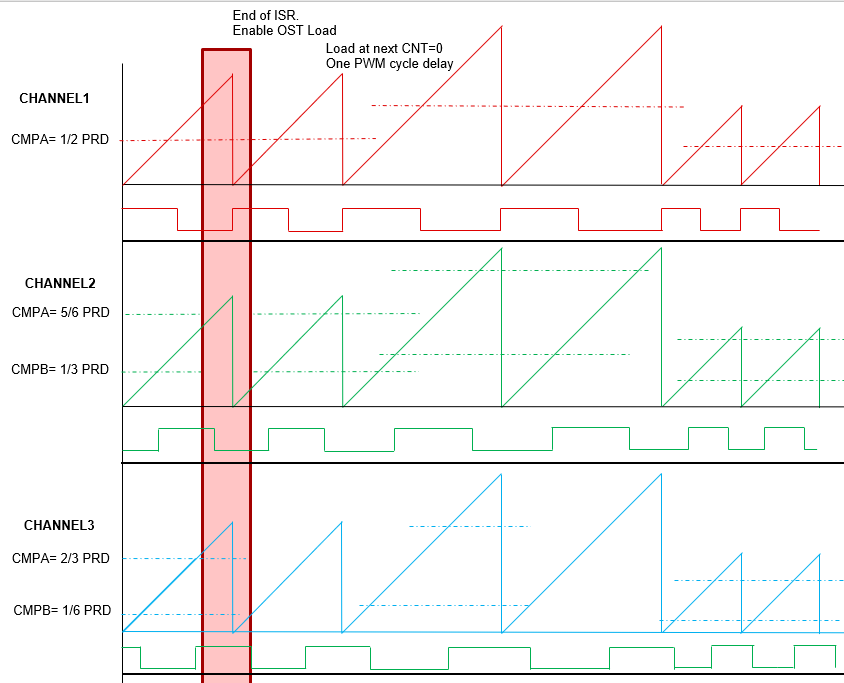
To achieve accurate control of load timing in multiple PWM modules, global and one-shot load features are leveraged. First, global load is configured separately in PWM 1/2/3 to make sure the period and comp A/B values are loaded simultaneously when CTR=0. Second, one-shot load is enabled, to make sure the value is loaded only after the control loop running is totally finished before the content in the shadow registers is loaded into the active registers.
 Figure 2-2 Primary Side PWM With
Frequency Change
Figure 2-2 Primary Side PWM With
Frequency ChangeAn example is shown in Figure 2-2 to explain why one-shot load is necessary. The special case to consider here is when the control ISR execution period is crossing two PWM periods. If loading to PRD and CMPA/B shadow register is not in the same PWM cycle, the phase shifting of phase B and C would be disordered. To avoid the mismatch, one-shot is enabled only at the end of the control ISR. As the result, the new PRD and CMPA/B value would become effective simultaneously at the next time base counter equal to zero match. Though this may bring a minor delay, which is less than a PWM cycle, it would ensure all the PWM channels work properly.
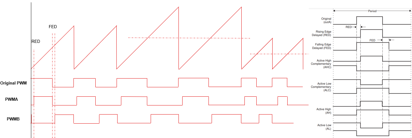
Normally, three-phase LLC works with a fixed 50% duty cycle, thus complimentary PWM signals are easy to generate with DB (dead-band) submodule in PWM. Figure 2-3 represents an example of Phase-A, where active-high complementary (AHC) mode is used to generate two complementary PWM signals. Similarly, the dead-band feature could be used to generate the complementary PWM for Phase-B and Phase-C.
 Figure 2-3 Primary Side Complementary
PWM
Figure 2-3 Primary Side Complementary
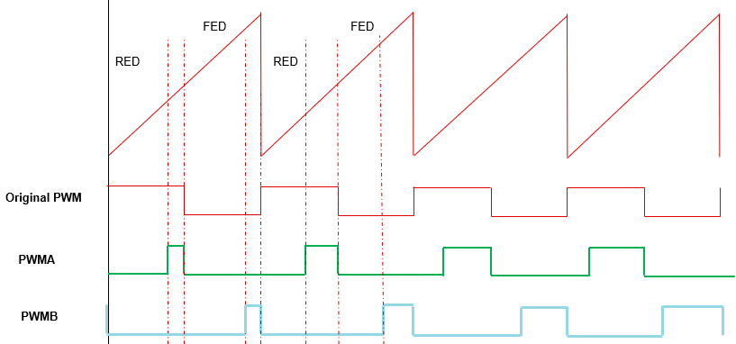
PWMUnder certain special circumstances, LLC may not work under a fixed 50% duty cycle. For example, during power on, the converter normally requires soft-starting where the PWM duty cycle increases step-by-step to avoid problems like current inrush and output voltage over-shoot. With PWM generating logic proposed above, dead-band could be used to adjust the duty-cycle.
During power on, the dead-band Rising edge delay (RED) and Falling edge delay (FED) are set to a large value (0.95*period) and the duty cycle of both PWMA and PWMB would be limited to 5%. With the output voltage establishing, RED and FED could be decreased cycle-by-cycle and eventually down to normal dead-band value. As the result, PWMA and PWMB duty cycle would increase slowly until reaching up to 50%. The process of soft-starting is shown in Figure 2-4.
 Figure 2-4 Leveraging Dead-Band to
Achieve Soft-Starting