SPRAD15 March 2022 TMS320F280021 , TMS320F280021-Q1 , TMS320F280023 , TMS320F280023-Q1 , TMS320F280023C , TMS320F280025 , TMS320F280025-Q1 , TMS320F280025C , TMS320F280025C-Q1 , TMS320F280033 , TMS320F280034 , TMS320F280034-Q1 , TMS320F280036-Q1 , TMS320F280036C-Q1 , TMS320F280037 , TMS320F280037-Q1 , TMS320F280037C , TMS320F280037C-Q1 , TMS320F280038-Q1 , TMS320F280038C-Q1 , TMS320F280039 , TMS320F280039-Q1 , TMS320F280039C , TMS320F280039C-Q1 , TMS320F280040-Q1 , TMS320F280040C-Q1 , TMS320F280041 , TMS320F280041-Q1 , TMS320F280041C , TMS320F280041C-Q1 , TMS320F280045 , TMS320F280048-Q1 , TMS320F280048C-Q1 , TMS320F280049 , TMS320F280049-Q1 , TMS320F280049C , TMS320F280049C-Q1 , TMS320F28075 , TMS320F28075-Q1 , TMS320F28076 , TMS320F28374D , TMS320F28375D , TMS320F28376D , TMS320F28377D , TMS320F28377D-EP , TMS320F28377D-Q1 , TMS320F28378D , TMS320F28379D , TMS320F28379D-Q1 , TMS320F28384D , TMS320F28384D-Q1 , TMS320F28384S , TMS320F28384S-Q1 , TMS320F28386D , TMS320F28386D-Q1 , TMS320F28386S , TMS320F28386S-Q1 , TMS320F28388D , TMS320F28388S , TMS320F28P550SJ , TMS320F28P559SJ-Q1 , TMS320F28P650DH , TMS320F28P650DK , TMS320F28P650SH , TMS320F28P650SK , TMS320F28P659DH-Q1 , TMS320F28P659DK-Q1 , TMS320F28P659SH-Q1
3.2 SR PWM Duty Limitation
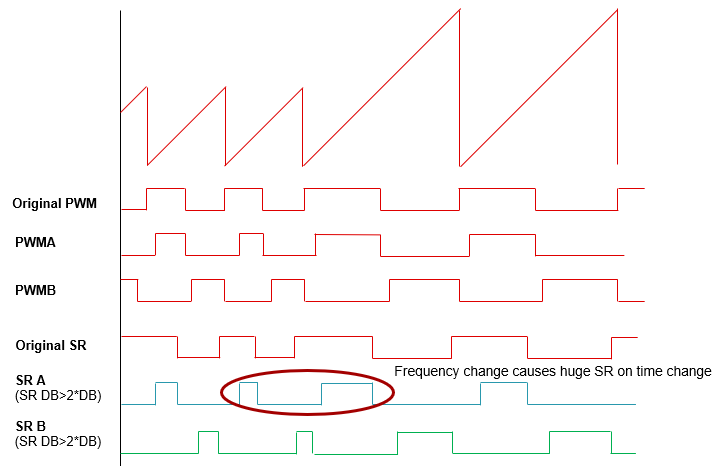
Figure 3-2 represents a working condition where SR on time exceeds the resonant period LLC converter. If the PWM cycle actually crosses 2 PWM counter cycles, it may cause some disorder on PWM waveform when there is a huge frequency change.
When PWM frequency is lower than the resonant frequency of LLC, the on-time of SR switch needs to be limited. Otherwise, a reverse current would exist on SR MOS which would significantly influence the efficiency of the converter and even bring the converter to danger due to the reverse recovery of the body-diode.
 Figure 3-2 Example of SR On-Time
Change
Figure 3-2 Example of SR On-Time
ChangeThe CLB module on Gen 3 C2000 devices makes it easy to achieve highly flexible PWM waveforms. CLB implementation of PWM on time limitation is shown in Figure 3-3.
 Figure 3-3 CLB Configuration
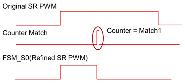
In this design, a counter is configured to limit the maximum on time of SR PWM. The counter would start to count once it receives the SR PWM rising edge and generate a pulse (match 1) when it reaches the configured match value. The match value decides maximum on time by CLB clock counts.
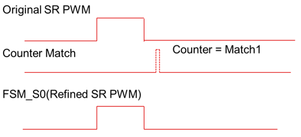
In LUT0, match signal is ‘ORed’ with input 2, which is the falling edge of original SR PWM, which is then connected into FSM_0. By correctly configuring FSM. e0 (rising edge of original PWM) would be able to pull high the S0 of FSM_S0, and e1 (falling edge of original PWM OR counter 0 match signal) would be able to pull down S0. By doing this, the S0 became the refined PWM which would be pulled down if the on-time exceeds the maximum value. The waveform of CLB internal signal is shown in Figure 3-4.

 Figure 3-4 CLB Internal Waveform
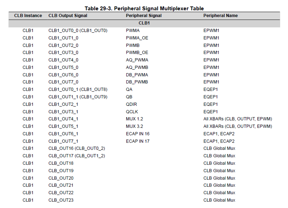
Finally, FSM_S0 could be the CLB ouput through OUTLUT, and finally reflect back as PWM output by configuring CLB output MUX.
 Figure 3-5 Multiple CLB Out is Connected
to Peripheral via Multiplexer
Figure 3-5 Multiple CLB Out is Connected
to Peripheral via MultiplexerFigure 3-6 shows the waveform when the PWM cycle is changing from 3 µs to 15 µs while the maximum on-time is limited to 5 µs. As the waveform shows, the refined PWM is pulled down immediately when the on time reaches 5 µs, thus this feature could be leveraged to limit the reverse current on SR FET in LLC convert.
 Figure 3-6 PWM Limitation