SPRADD4 October 2023 AM625SIP
6 Floorplan Component Placement
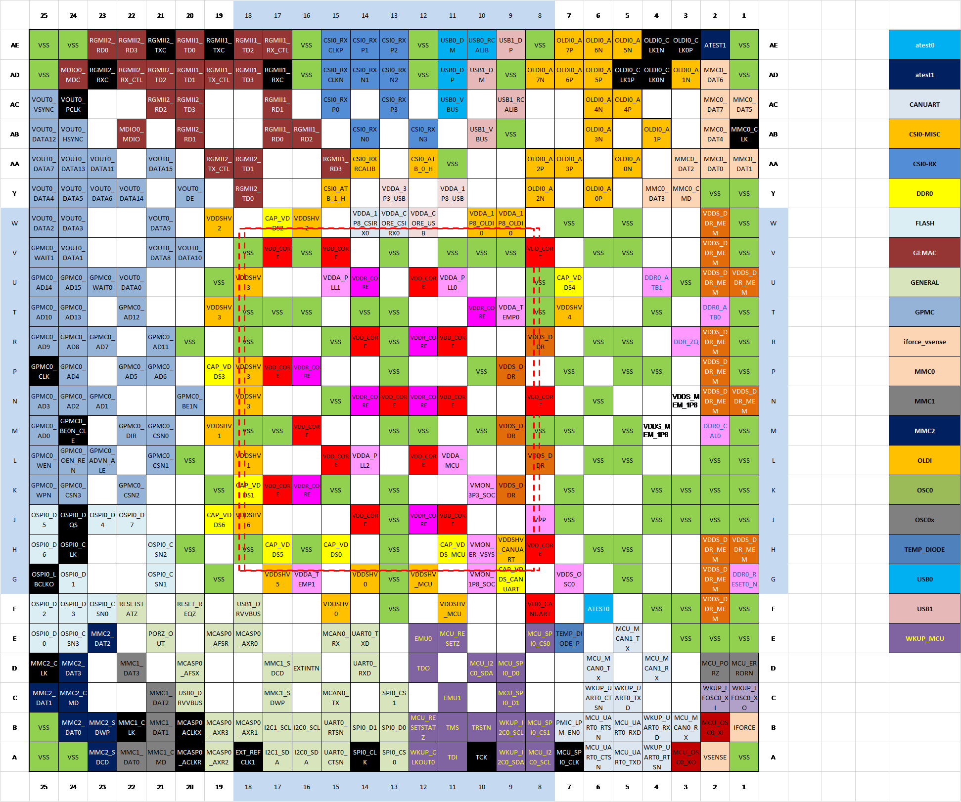
Careful analysis is required to analyze the locations of the interfaces used on the device and the associated components and connectors. Optimum trace routing will have routes as short as possible with a minimum cross-over. The AM62xSiP offers interface selection flexibility through pin-mux choices. Pin-muxing enables a same interface function made available on multiple pins and is selectable through a pin mux option. Favorable pin-mux options that ease PCB routing and component placement can be fully utilized to further optimize the PCB design. The figure below shows the default arrangement of the signal balls and the power and ground balls. Priority is given to component placements without pin-mux options such as CSI, USB, OLDI/LVDS, and so forth.
 Figure 6-1 AM62xSiP Floorplan