SPRUJ73 December 2023
2.5.2 LIN
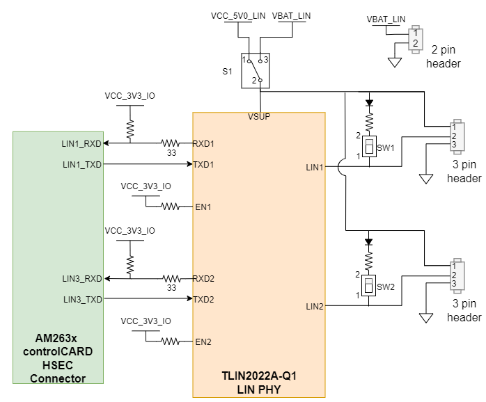
The AM263x controlCARD Docking Station supports Local Interconnect Network communication through the use of a Dual LIN transceiver (TLIN2022A-Q1) that outputs the LIN Bus channels LIN1 and LIN3 of the AM263x SoC to the second pin of a pair of 3 pin headers.
 Figure 2-8 LIN Transceiver
The LIN transceiver has power input VSUP, the device supply voltage. The AM263x SoC LIN1 data transmit data input is mapped to TXD1 of the transceiver and the AM263x SoC LIN3 data transmit data input is mapped to TXD2 of the transceiver. The LIN receive data output of the transceiver RXD1 is mapped to the LIN1 RX signal of the AM263x SoC and the data output of the transceiver RXD2 is mapped to the LIN3 RX signal of the AM263x SoC. Both RXD1 and RXD2 nets have a series termination resistor close to the transceiver.
The AM263x SoC does not have an integrated pull up for the LIN RX signal and therefore an external pull up resistor is needed to the I/O supply voltage.
The AM263x controlCARD Docking Station includes a single pole double throw switch (S1) to control the voltage supply for the LIN Transceiver.
| LIN Voltage Switch Position (S1) | Voltage Supply |
|---|---|
| Pin 1-2 | VMAIN, 5V supply output from the USB-C connection |
| Pin 2-3 | VBAT_LIN, external voltage supply from pin 1 of 2 pin header |
| LIN Node Application Switch Position (SW1, SW2) | LIN Node Application |
|---|---|
| Pin 1 | Device node application |
| Pin 2 | Controller node application |