SSZT498 april 2019 SN74AXC1T45

“The Matrix” showed a dystopian world where the human race was trapped in a computer simulation. In the movie, the phrase “a glitch in the matrix” described the feeling of déjà vu – experiencing something that doesn’t quite match with what we know about reality.
In electronic systems, signal glitches can and do result in a range of responses, from abnormal behavior to outright failure.
Signal glitches often arise due to the unexpected behavior of circuit implementations used to create a system’s overall signal chain. This unexpected behavior is often the result of a confluence of factors between the integrated circuits (ICs) that make up the signal chain and the various operating modes that the system transitions through in the course of normal operation.
Given the nature of signal glitches, pinpointing their root cause is often difficult, especially for complex systems. Often, the first place that signal glitches occur is during power up, as different subsystems ramp up to their known, stable power-up states. Signal glitches during power up often occur between the output and input pins of circuits within a system or subsystem. The result will be an abnormal boot up and potentially failure during power up.
Designers often turn to complex power-sequencing implementations to stagger the power up of certain subsystems or circuits in order to avoid signal glitches. These implementations often result in longer boot-up times, more complicated software and additional costs.
One simple way to avoid signal glitches during power up is to use building-block ICs that won’t have glitches during power-supply ramp-up. Level-translator devices common in most signal chains enable voltage-level shifting between the input and output pins of devices that reside on two different voltage nodes. Selecting level translators designed to support glitch-free power up can go a long way in preventing signal glitches and avoiding the need for complex power-sequencing schemes.
TI’s latest SN74AXC family of direction-controlled level translators are specifically designed and tested to not have signal glitches, enabling you to avoid complicated power-sequencing schemes that other level translators may require.
One way to test the robustness of a level translator against signal glitches is to perform power-up testing of the device using a combination of different voltage ramp-up rates (volts per second) at different voltage rails supported by the two interfacing devices , VCCA and VCCB points, while varying the direction of voltage ramp between VCCA and VCCB. This type of test captures many of the different permutations of input and output signals that a voltage translator is likely to encounter during power up.
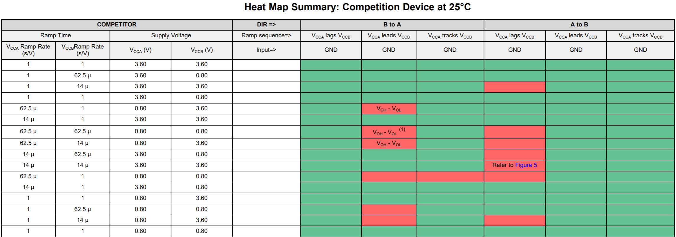
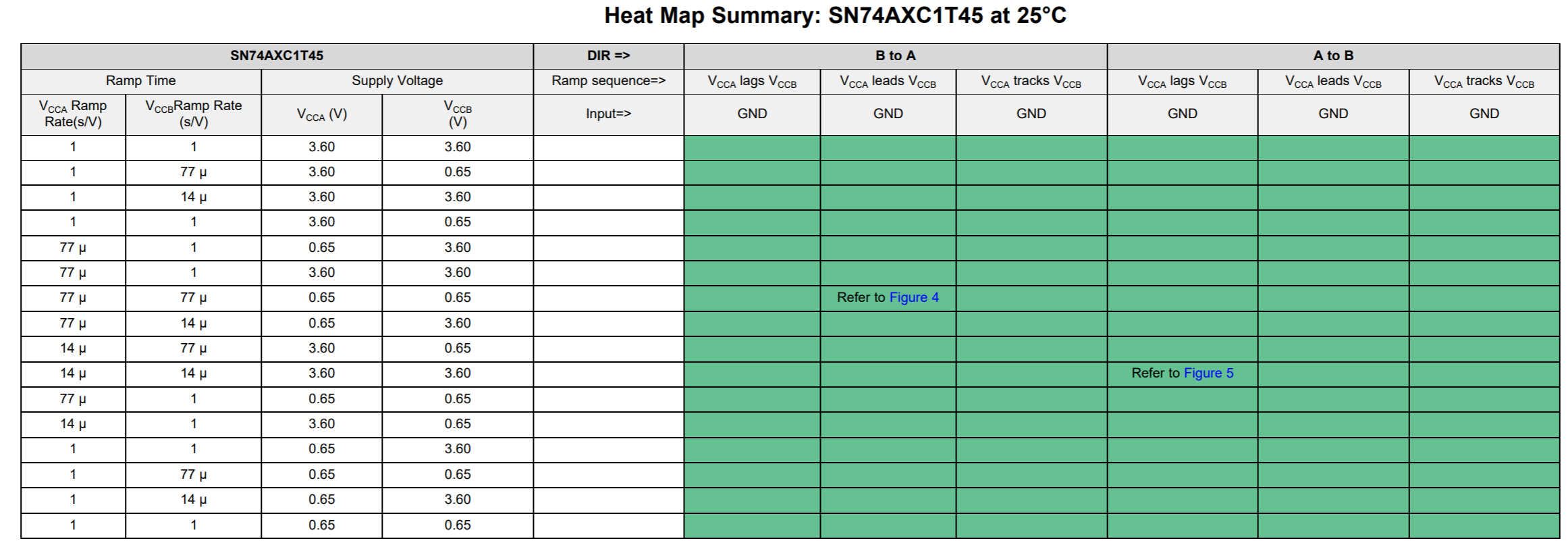
When it comes to glitch-free power up, the robustness of TI’s SN74AXC level translators is apparent in power-up testing results that compare the glitch performance of TI’s SN74AXC1T45 (a one-bit level translator) to a competing device with the same footprint and functionality. Figure 1 and Figure 2 show the results of glitch testing for different combinations of voltage ramp-up rates (volts per second) at different VCCA and VCCB points with different ramp directions between VCCA and VCCB. The red cells denote a glitch.
 Figure 1 Glitch Heat Map for a
Competing Device at 25°C
 Figure 2 Glitch Heat Map for TI’s
SN74AXC1T45 at 25°C
Figure 2 Glitch Heat Map for TI’s
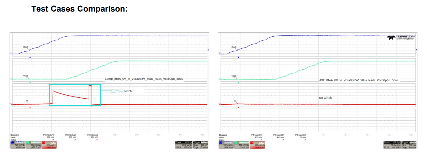
SN74AXC1T45 at 25°CThe heat map shows the competing device with multiple glitches, while the same set of tests on the SN74AXC1T45 resulted in no glitches. Two of the test cases (Figure 3 and Figure 4) show the magnitude of the glitch for a given VCCA (blue) and VCCB (teal) ramp profile.
 Figure 3 Glitch Testing Case of a
Competing Device (Left) and the SN74AXC1T45 (Right) with a 50-Μs Ramp Rate and
0-v Input
 Figure 4 Glitch Testing Case of a
Competing Device (Left) and the SN74AXC1T45 (Right) with 1-s/Vramp Rate and 0-v
Input
Figure 4 Glitch Testing Case of a
Competing Device (Left) and the SN74AXC1T45 (Right) with 1-s/Vramp Rate and 0-v
InputSignal glitches, especially during power up, often require a great deal of engineering time to debug, which most development schedules don’t account for. Using building-block devices like AXC level translators from TI not only helps avoid catastrophic failures during operation, but can save engineering time and resources during development, leading to a better return on investment.
You don’t have to be the “the One” to root out glitches that may be lurking in your design. You just need to select devices like level translators that are designed to operate glitch-free.
Additional Resources
- The Glitch Free Power Sequencing With AXC Level Translators application note provides a more detailed look at the glitch performance of TI’s AXC level translators over a range of power-sequencing ramp-up profiles.
- Learn more about voltage level translation.